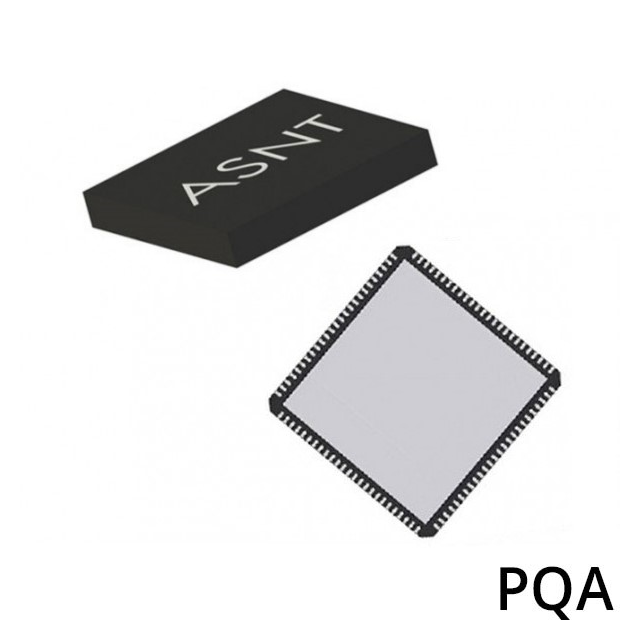
ADSANTEC ASNT2016-PQA


- Part Number:
ASNT2016-PQA
- Manufacturer:
- Category:
- RoHs:
 RoHS Compliant
 - Datasheet:
 ASNT2016-PQA_Datesheet
 - Description:
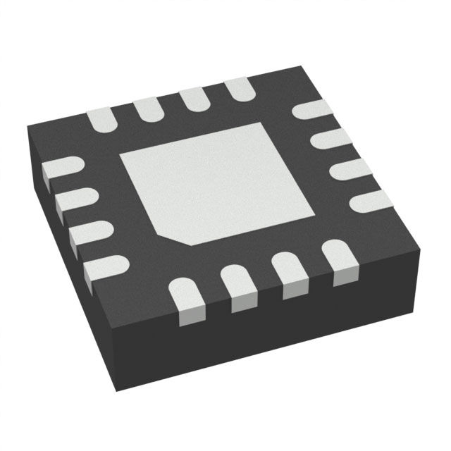
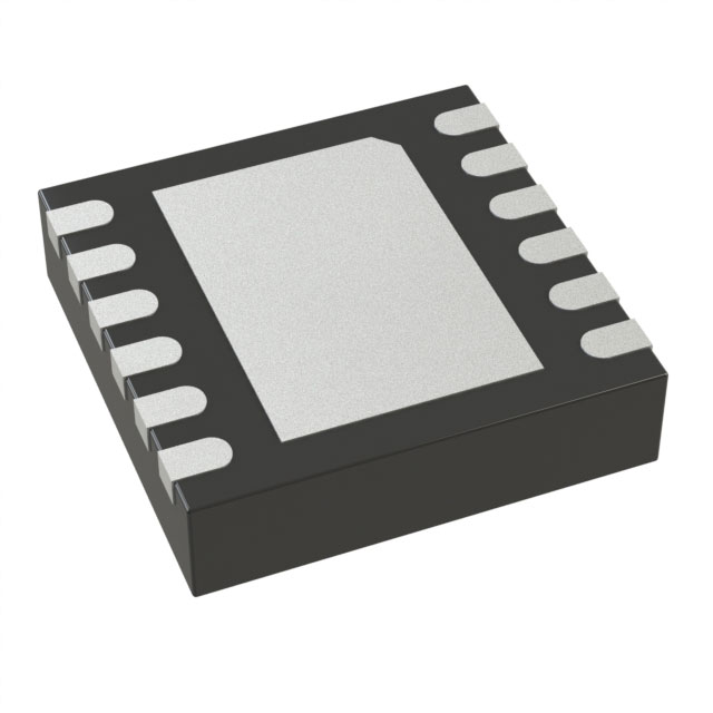
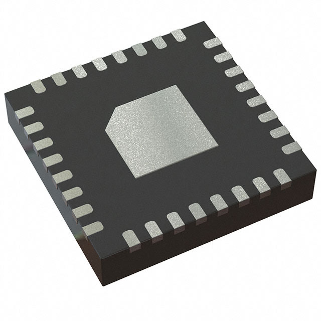
IC CLK DEMULTI 1:16 100QFN
- In stock 73

DESCRIPTION
· The ASNT2016-PQA (ASNT2042) is a 1:16 demultiplexer (DMUX) with an integrated full-rate clock and data recovery (CDR) unit.
· It supports data rates from 11.3 to 12.5 Gbps in CDR mode and can operate up to 12.5 Gbps in broadband digital mode with a full-rate clock.
· The device supports both RZ and NRZ input data formats and features LVDS output buffers with a low-power proprietary architecture.
· It provides a stable clock-divided-by-16 LVDS output with 90°-step phase selection and supports clock-divided-by-16/64 input reference clock.
· The ASNT2016-PQA operates on a single +3.3 V power supply and is designed for industrial temperature ranges.
· It consumes low power, specifically 730 mW at 12.5 Gbps, and is available in a standard 100-pin QFN package measuring 12 mm x 12 mm.
FEATURES
· Integrated 1:16 DMUX with full-rate CDR.
· Supports data rates from 11.3 to 12.5 Gbps.
· Operates in broadband digital mode up to 12.5 Gbps.
· Compatible with RZ and NRZ input data formats.
· Features LVDS output buffers with low-power architecture.
· Provides stable clock-divided-by-16 LVDS output with 90°-step phase selection.
· Supports clock-divided-by-16/64 input reference clock.
· Single +3.3 V power supply.
· Industrial temperature range.
· Low power consumption of 730 mW at 12.5 Gbps.
· Available in a 100-pin QFN package (12 mm x 12 mm).
APPLICATIONS
· High-speed data communication systems.
· Optical networking equipment.
· Data center infrastructure.
· Broadband digital signal processing.
· Industrial and telecommunications applications requiring precise clock recovery and data demultiplexing.
Purchase
No need to register to order from JMBom Electronics, but signing in lets you track your order like a pro. Give it a try for a smoother shopping ride.
Means
Easy peasy! Pay your way with PayPal, Credit Card, or wire transfer in USD. We've got you covered.
RFQ(Request for Quotations)
Get the freshest prices and stock updates by asking for a quote! Our sales team will shoot you an email within a day. It's that simple.
IMPORTANT NOTICE
1. Look out for your order details in your inbox! (If it's missing, check the spam folder just in case.)
2. Our sales manager will double-check the order and keep you posted on any price or stock changes. No worries, we've got you covered.

Shipping Rate
We ship orders once a day around 5 p.m., except Sunday. Once shipped, the estimated delivery time depends on the courier company you choose, usually 5-7 working days.

Shipping Methods
We provide DHL, FedEx, UPS, EMS, SF Express, and Registered Air Mail international shipping.


Payment
You can pay the orders on the website directly or pay by wire transfer offline. We support: Paypal、VISA、Credit Card.