
Infineon Technologies IR22771SPBF


- Part Number:
IR22771SPBF
- Manufacturer:
- Category:
- RoHs:
 RoHS Compliant
 - Datasheet:
 IR22771SPBF_Datesheet
 - Description:
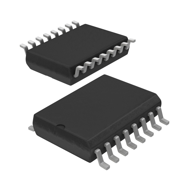
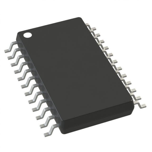
IC CURRENT SENSE 16SOIC
- In stock 0

IR22771SPBF Datasheet Summary
Overview
The IR22771SPBF is a high voltage, high speed, single phase current sensor interface designed for AC motor drive applications. It features a floating channel up to 600V, synchronous sampling measurement system, and high PWM noise rejection capability. The device is suitable for bootstrap power supplies and offers low sensing latency.
Features
- Floating Channel Voltage: Up to 600V
- Synchronous Sampling Measurement System: Ensures accurate current sensing
- High PWM Noise Rejection: Effective ripple rejection
- Digital PWM Output: Suitable for high-speed applications
- Fast Over Current Detection: Provides protection for IGBTs
- Low Sensing Latency: Less than 7.5 µsec at 20kHz PWM frequency
- Package Type: SOIC16WB
Electrical Characteristics
- Input Voltage Range: ±250mV
- Bootstrap Supply Range: 8-20V
- Quiescent Current: 2.2 mA (max) for floating channel
- Sensing Latency: Less than 7.5 µsec at 20kHz PWM frequency
- Throughput: 40 ksample/sec (max) at 20kHz PWM frequency
- Over Current Threshold: ±470 mV (max)
Absolute Maximum Ratings
- High Side Floating Supply Voltage (VB): -0.3 to 625V
- High Side Floating Ground Voltage (VS): VB - 25V to VB + 0.3V
- High-Side Input Voltages (Vin+/Vin-): VB - 5V to VB + 0.3V
- High-Side Range Selectors (G0/G1): VB - 0.3V to VB + 0.3V
- Low-Side Fixed Supply Voltage (VCC): -0.3 to 25V
- Synchronization Signal (Sync): -0.3V to VCC + 0.3V
- PWM Output (PO): -0.3V to VCC + 0.3V
- Over Current Output (OC): -0.3V to VCC + 0.3V
- Maximum Power Dissipation: 250 mW
- Thermal Resistance (RthJA): 90 °C/W
- Operating Junction Temperature (TJ): -40 to 125 °C
- Storage Temperature (TS): -55 to 150 °C
Recommended Operating Conditions
- High Side Floating Supply Voltage (VBS): VS + 8.0V to VS + 20V
- High Side Floating Ground Voltage (VS): -5V to 600V
- High-Side Input Voltages (Vin+/Vin-): VS - 5.0V to VS + 5.0V
- Low-Side Logic Fixed Supply Voltage (VCC): 8V to 20V
- Synchronization Signal Frequency (fsync): 4kHz to 20kHz
- Ambient Temperature (TA): -40 to 125 °C
Static Electrical Characteristics
- Quiescent VBS Supply Current (IQBS): 1 to 2.2 mA
- Quiescent VCC Supply Current (IQCC): 6 mA
- Offset Supply Leakage Current (ILK): 50 µA (max)
- Maximum Input Voltage Before Saturation (Vinmax): 250 mV
- Minimum Input Voltage Before Saturation (Vinmin): -250 mV
- Sync Input High Threshold (VIH): 2.2V
- Sync Input Low Threshold (VIL): 0.8V
- Sync Input Hysteresis (Vhy): 0.2V
- Over Current Activation Threshold (|Vocth|): 300 to 470 mV
AC Electrical Characteristics
- PWM Frequency (fsync): 4kHz to 20kHz
- Throughput (fout): 2 * fsync ksample/sec
- Bandwidth (BW): fsync kHz
- Group Delay (GD): 4 * fsync to 1 µs
- Minimum Duty Cycle (Dmin): 10%
- Maximum Duty Cycle (Dmax): 30%
- De-bounce Time of OC (tdOCon): 2.7 to 4.7 µs
- Time to Reset OC Forcing PO (TOCoff): 0.5 µs
- Measurement Delay (MD): 2 * fsync to 30 µs
- Step Response (SR): fsync to 51 µs
Pin Configuration
- 1: VCC (Low side voltage supply)
- 2: NC (No connection)
- 3: VSS (Low side ground supply)
- 4-5: NC (No connection)
- 6: OC (Over current signal, open drain)
- 7: PO (PWM output, open drain)
- 8: Sync (DSP synchronization signal)
- 9-10: NC (No connection)
- 11: G0 (Integrator gain lsb)
- 12: G1 (Integrator gain msb)
- 13: VS (High side return)
- 14: VIN- (Negative sense input)
- 15: VIN+ (Positive sense input)
- 16: VB (High side supply)
Functional Description
- SYNC Input: Clocks the whole device and must be synchronous with the triangular PWM carrier.
- PWM Output (PO): Open collector output (active low) that must be pulled up with an external resistor.
- Over Current Output (OC): Open drain output (active low) that triggers when the input voltage exceeds the threshold.
- DC Transfer Function: The PWM output duty cycle is inversely proportional to the input signal.
- Filter AC Characteristics: The signal path includes three stages, with the first two stages performing filtering actions to reject PWM noise.
Sizing Tips
- Bootstrap Supply: The VBS supply is floating and can be generated using a bootstrap method with a diode and capacitor.
- Bootstrap Capacitor Sizing: Consider factors such as quiescent current, leakage current, and charge required by internal level shifters.
- Bootstrap Diode: Should have a high breakdown voltage (BV) and fast recovery time (trr < 100 ns).
Purchase
No need to register to order from JMBom Electronics, but signing in lets you track your order like a pro. Give it a try for a smoother shopping ride.
Means
Easy peasy! Pay your way with PayPal, Credit Card, or wire transfer in USD. We've got you covered.
RFQ(Request for Quotations)
Get the freshest prices and stock updates by asking for a quote! Our sales team will shoot you an email within a day. It's that simple.
IMPORTANT NOTICE
1. Look out for your order details in your inbox! (If it's missing, check the spam folder just in case.)
2. Our sales manager will double-check the order and keep you posted on any price or stock changes. No worries, we've got you covered.

Shipping Rate
We ship orders once a day around 5 p.m., except Sunday. Once shipped, the estimated delivery time depends on the courier company you choose, usually 5-7 working days.

Shipping Methods
We provide DHL, FedEx, UPS, EMS, SF Express, and Registered Air Mail international shipping.


Payment
You can pay the orders on the website directly or pay by wire transfer offline. We support: Paypal、VISA、Credit Card.


Infineon Technologies
Infineon Technologies
Infineon Technologies
Infineon Technologies
Infineon Technologies
Infineon Technologies
Infineon Technologies
Infineon Technologies
Infineon Technologies
Infineon Technologies
Infineon Technologies
Infineon Technologies