
Richtek USA Inc. RT6362GFP


- Part Number:
RT6362GFP
- Manufacturer:
- Category:
- RoHs:
 RoHS Compliant
 - Datasheet:
- Description:
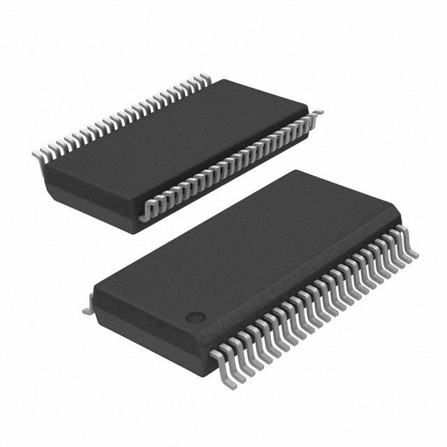
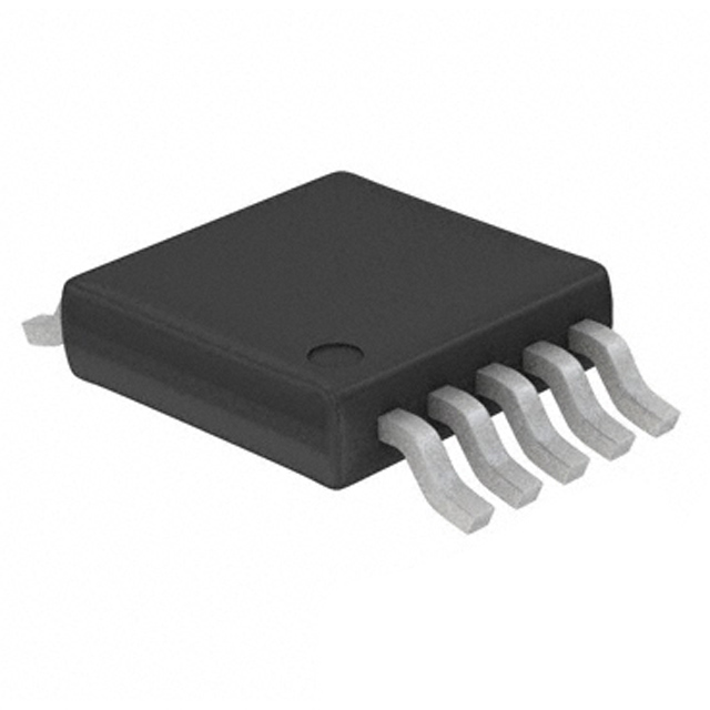
IC REG BUCK ADJ 2.5A 10MSOP
- In stock 3,195

Model Information: RT6362GFP
General Description
The RT6362GFP is a high-efficiency, asynchronous step-down converter designed for applications requiring a wide input voltage range and low quiescent current. It features peak current mode control and is capable of operating with input voltages from 4V to 60V. The device can program the output voltage between 0.8V to VIN, making it suitable for a variety of power systems.
Features
- Wide Input Voltage Range: 4.5V to 60V (Soft-start finished)
- Wide Output Voltage Range: 0.8V to VIN
- Reference Accuracy: ±1.5%
- Peak Current Mode Control
- Integrated 150mΩ High-Side MOSFET
- Low Quiescent Current: 90μA
- Low Shutdown Current: 1.3μA
- Adjustable Switching Frequency: 100kHz to 2.5MHz
- Synchronizable Switching: 300kHz to 2.2MHz
- Power Saving Mode (PSM) at Light Load
- Low Dropout at Light Loads with Integrated Boot Recharge FET
- Externally Adjustable Soft-Start
- Power Good Indication
- Enable Control
- Adjustable UVLO Voltage and Hysteresis
- Built-In UVLO, UVP, OVP, OCP, OTP
Applications
- 12V, 24V, and 48V Power Systems
- GPS, Entertainment Systems
- Telecom, Computer, Industrial, and Consumer Electronics
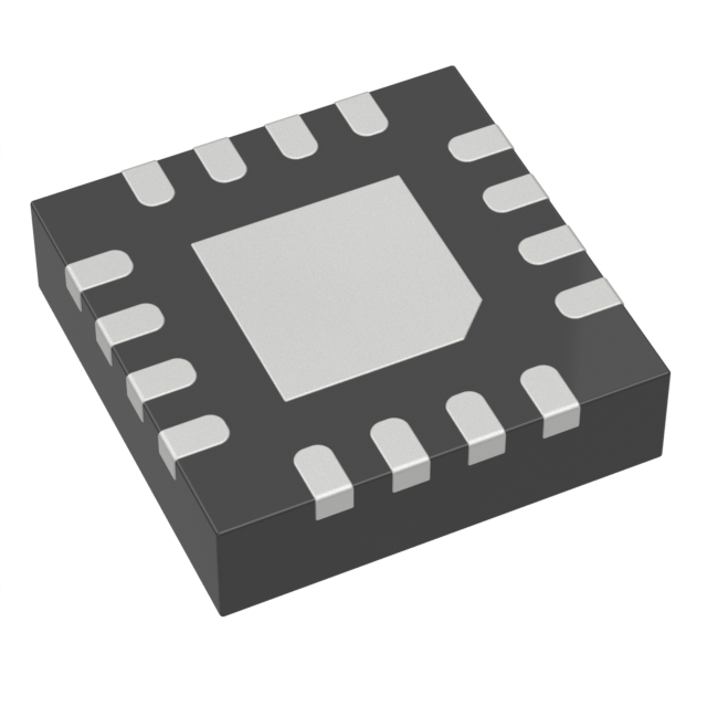
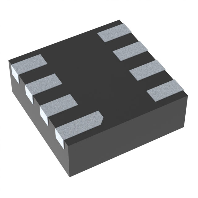
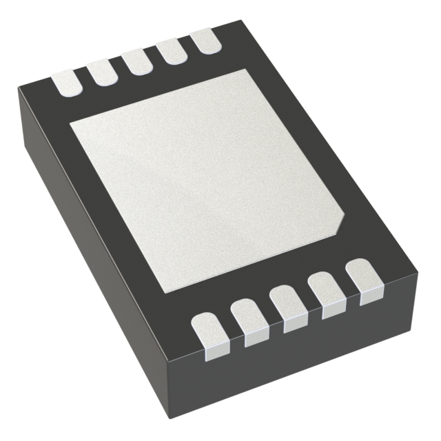
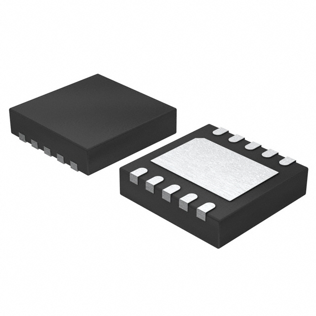
Pin Configuration (Top View)
| Pin No. | Pin Name | Function | SOP-8 (Exposed Pad) | WDFN-10SL 3x3 | MSOP-10 (Exposed Pad) |
|---|---|---|---|---|---|
| 1 | BOOT | Bootstrap capacitor connection node to supply the high-side gate driver. | 1 | 1 | 1 |
| 2 | VIN | Power input. Input voltage range is from 4V to 60V. | 2 | 2 | 2 |
| 3 | EN | Enable control pin with internal pull-up current source. | 3 | 3 | 3 |
| 4 | SS/TR | Soft-start and tracking control input. | -- | 4 | 4 |
| 5 | RT/SYNC | Frequency setting and external synchronous signal input. | 4 | 5 | 5 |
| 6 | PGOOD | Open-drain power-good indication output. | -- | 6 | 6 |
| 7 | FB | Output voltage sense. | 5 | 7 | 7 |
| 8 | COMP | Compensation node. | 6 | 8 | 8 |
| 9 | GND | Ground. | 7 | 9 | 9 |
| 10 | SW | Switch node. | 8 | 10 | 10 |
| -- | PAD | Exposed pad for thermal dissipation. | -- | 11 | 11 |
Functional Block Diagram
- UVLO: Under-Voltage Lockout
- OVP: Over-Voltage Protection
- UVP: Under-Voltage Protection
- OCP: Over-Current Protection
- OTP: Over-Temperature Protection
- PGOOD: Power-Good Indication
- FB: Feedback for output voltage sensing
- SS/TR: Soft-start and tracking control
- COMP: Compensation node for loop stability
- RT/SYNC: Frequency setting and synchronization input
- EN: Enable control
- VIN: Power input
- BOOT: Bootstrap capacitor connection
- SW: Switch node for output power
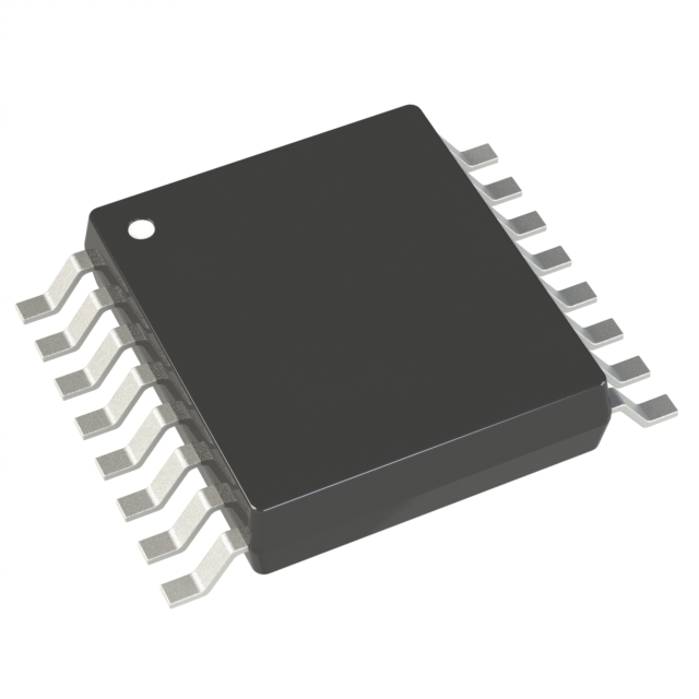
Ordering Information
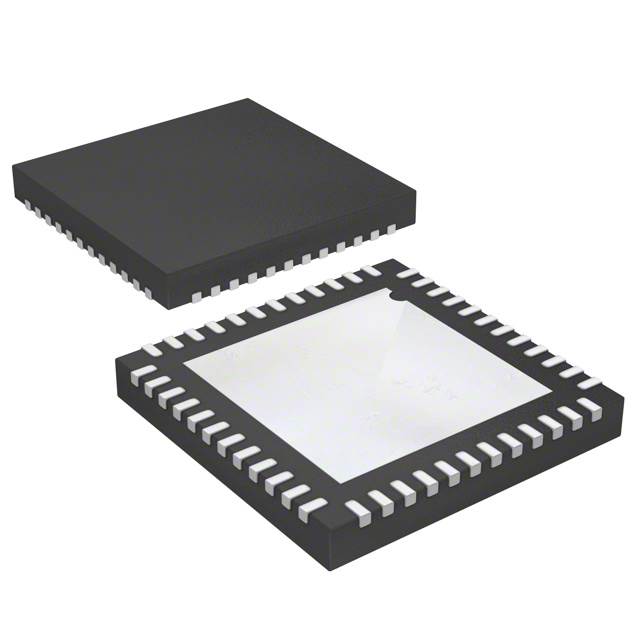
- Package Type: MSOP-10 (Exposed Pad)
- Lead Plating System: Green (Halogen Free and Pb Free)
- Marking Information: RT6362GFP, Date Code (YMDNN)
Thermal Information
- Thermal Resistance (θJA): 31.2°C/W (JEDEC standard)
- Thermal Resistance (θJC - Top): 87.9°C/W
- Thermal Resistance (θJC - Bottom): 2.1°C/W
Absolute Maximum Ratings
- Supply Voltage (VIN): -0.3V to 65V
- Enable Voltage (EN): -0.3V to 65V
- Switch Voltage (SW): -0.6V to 65V
- BOOT to SW Voltage: -0.3V to 6V
- All Other Pins: -0.3V to 6V
- Lead Temperature (Soldering, 10 sec.): 260°C
- Junction Temperature: 150°C
- Storage Temperature Range: -65°C to 150°C
Recommended Operating Conditions
- Supply Input Voltage (VIN): 4V to 60V
- Output Voltage: 0.8V to VIN
- Junction Temperature Range: -40°C to 125°C
Electrical Characteristics (VIN = 12V, TA = TJ = 25°C)
- Input Operating Voltage (VIN): 4V to 60V
- VIN Under-Voltage Lockout Threshold (VUVLOH): 4.1V to 4.5V (rising), 3.8V to 4V (falling)
- Shutdown Current (ISHDN): 1.3μA (max)
- Quiescent Current (IQ): 90μA (typ)
- Enable Threshold Voltage (VTH_EN): 1.15V to 1.36V
- Pull-Up Current (IEN): 0.9μA (typ)
- Hysteresis Current (IEN_Hys): 2.9μA (typ)
- Reference Voltage (VREF): 0.788V to 0.812V
- High-Side Switch On-Resistance (RDS(ON)_H): 150mΩ (max)
- Error Amplifier Transconductance (gm): 310μA/V (typ)
- Current Limit (ILIM): 3.825A to 5.175A
Package Dimensions
- MSOP-10 (Exposed Pad)A: 4.801mm to 5.004mmB: 3.810mm to 4.000mmC: 1.346mm to 1.753mmD: 0.330mm to 0.510mmF: 1.194mm to 1.346mmH: 0.170mm to 0.254mmI: 0.000mm to 0.152mmJ: 5.791mm to 6.200mmM: 0.406mm to 1.270mmX: 2.000mm to 2.300mmY: 2.000mm to 2.300mm (Option 1), 3.000mm to 3.500mm (Option 2)
Layout Guidelines
- Four-layer or six-layer PCB with maximum ground plane is strongly recommended for good thermal performance.
- Keep the traces of the main current paths wide and short.
- Place high-frequency decoupling capacitor CIN3 as close to the IC as possible to reduce loop impedance and minimize switch node ringing.
- Place bootstrap capacitor, CBOOT, as close to the IC as possible. Routing the trace with a width of 20mil or wider.
- Place multiple vias under the device near VIN and GND, and close to input capacitors to reduce parasitic inductance and improve thermal performance.
- The high-frequency switching nodes, SW and BOOT, should be as small as possible. Keep analog components away from the SW and BOOT nodes.
- Place freewheel diode, D1, and inductor, L1, as close to the IC as possible to reduce the area size of the SW exposed copper to reduce electrically coupling from this voltage.
Purchase
No need to register to order from JMBom Electronics, but signing in lets you track your order like a pro. Give it a try for a smoother shopping ride.
Means
Easy peasy! Pay your way with PayPal, Credit Card, or wire transfer in USD. We've got you covered.
RFQ(Request for Quotations)
Get the freshest prices and stock updates by asking for a quote! Our sales team will shoot you an email within a day. It's that simple.
IMPORTANT NOTICE
1. Look out for your order details in your inbox! (If it's missing, check the spam folder just in case.)
2. Our sales manager will double-check the order and keep you posted on any price or stock changes. No worries, we've got you covered.

Shipping Rate
We ship orders once a day around 5 p.m., except Sunday. Once shipped, the estimated delivery time depends on the courier company you choose, usually 5-7 working days.

Shipping Methods
We provide DHL, FedEx, UPS, EMS, SF Express, and Registered Air Mail international shipping.


Payment
You can pay the orders on the website directly or pay by wire transfer offline. We support: Paypal、VISA、Credit Card.


Richtek USA Inc.
Richtek USA Inc.

Richtek USA Inc.
Richtek USA Inc.
Richtek USA Inc.
Richtek USA Inc.
Richtek USA Inc.
Richtek USA Inc.
Richtek USA Inc.
Richtek USA Inc.
Richtek USA Inc.
Richtek USA Inc.