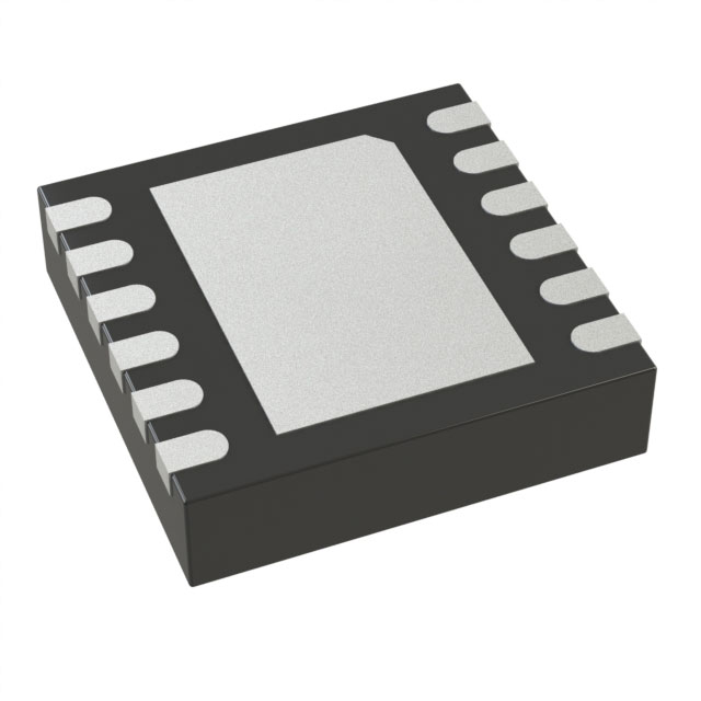
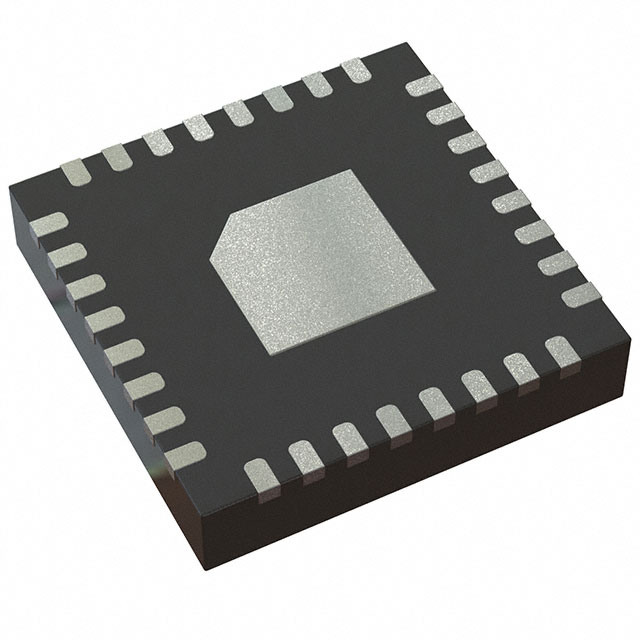
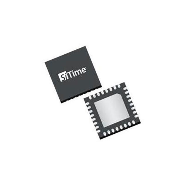
SiTime SIT92211AI


- Part Number:
SIT92211AI
- Manufacturer:
- Category:
- RoHs:
 RoHS Compliant
 - Datasheet:
 SIT92211AI_Datesheet
 - Description:
-40C TO 85C, 48PIN, 7070, 1.8V-3
- In stock 0

DESCRIPTION
· The SiT92211 is a 2.1 GHz, 10-output low-jitter clock fan-out buffer designed for high-frequency clock/data distribution and level translation.
· It supports primary, secondary, or crystal clock inputs, with primary and secondary sources accepting single-ended or differential signals.
· The selected clock is distributed to two output banks (A, B) and one LVCMOS output.
· Crystal input supports 8 MHz to 50 MHz crystals or single-ended clocks.
· Output drivers can be independently programmed to LVPECL, LVDS, HCSL, or HIZ mode.
· The LVCMOS output is synchronized and can be enabled/disabled glitch-free.
· Operates with a 3.3 V/2.5 V core supply and three independent 3.3 V/2.5 V output supplies.
· LVCMOS output can operate at 1.8 V.
FEATURES
· Additive jitter performance of 55 fs RMS.
· 3:1 input clock selection.
· Two universal clock inputs support up to 2.1 GHz and accept LVPECL, LVDS, LVCMOS, CML (AC-coupled), HCSL, SSTL, or single-ended clocks.
· Crystal input supports 8 MHz to 50 MHz crystals or single-ended clocks.
· Two output banks (A, B) can be programmed to LVPECL, LVDS, HCSL, or HIZ mode.
· Typical output skew of 30 ps.
· Level translation with 3.3 V/2.5 V core and output supplies.
· LVCMOS output operates at 3.3 V/2.5 V/1.8 V.
· Pin-controlled operation.
· High PSRR: -70 dBc (LVPECL), -73 dBc (LVDS).
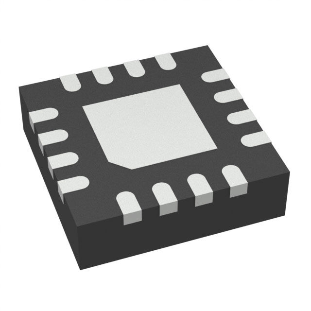
· Available in a 48-pin, 7mm x 7mm QFN package.
· Supports PCIe Gen1 to Gen5.
APPLICATIONS
· High-frequency clock distribution in low-jitter systems.
· Level translation for clock and data signals.
· Applications requiring precise clock synchronization.
· PCIe Gen1 to Gen5 compliant systems.
· Systems with mixed signal level requirements.
Purchase
No need to register to order from JMBom Electronics, but signing in lets you track your order like a pro. Give it a try for a smoother shopping ride.
Means
Easy peasy! Pay your way with PayPal, Credit Card, or wire transfer in USD. We've got you covered.
RFQ(Request for Quotations)
Get the freshest prices and stock updates by asking for a quote! Our sales team will shoot you an email within a day. It's that simple.
IMPORTANT NOTICE
1. Look out for your order details in your inbox! (If it's missing, check the spam folder just in case.)
2. Our sales manager will double-check the order and keep you posted on any price or stock changes. No worries, we've got you covered.

Shipping Rate
We ship orders once a day around 5 p.m., except Sunday. Once shipped, the estimated delivery time depends on the courier company you choose, usually 5-7 working days.

Shipping Methods
We provide DHL, FedEx, UPS, EMS, SF Express, and Registered Air Mail international shipping.


Payment
You can pay the orders on the website directly or pay by wire transfer offline. We support: Paypal、VISA、Credit Card.