NXP ADC1213D080HN/C1/5


- Part Number:
ADC1213D080HN/C1/5
- Manufacturer:
- Category:
- RoHs:
 RoHS Compliant
 - Datasheet:
 ADC1213D080HN/C1/5_Datesheet
 - Description:
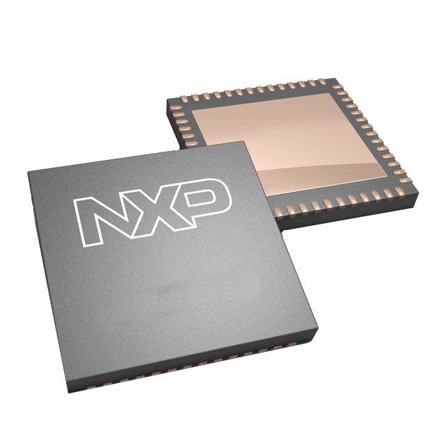
IC ADC 12BIT PIPELINED 56HVQFN
- In stock 0

DESCRIPTION
· The ADC1213D is a dual-channel 12-bit ADC optimized for high dynamic performance and low power consumption, supporting sample rates up to 125 Msps.
· It features a pipelined architecture with output error correction, ensuring accuracy and zero missing codes across its operating range.
· Powered by a 3 V analog source and a 1.8 V output driver, it includes two differential serial outputs compliant with the JESD204A standard.
· Configuration is facilitated via an integrated SPI and binary level control pins at power-up.
· Offers a programmable full-scale SPI for flexible input voltage ranges from 1 V to 2 V peak-to-peak.
· Maintains excellent dynamic performance up to input frequencies of 170 MHz, suitable for communications, imaging, and medical applications.
FEATURES
· Dual 12-bit ADC with sample rates of 65 Msps, 80 Msps, 105 Msps, or 125 Msps.
· SNR of 70 dBFS and SFDR of 86 dBc.
· Input bandwidth of 600 MHz.
· Power dissipation of 995 mW at 80 Msps.
· Features a clock input divided by 2 to reduce jitter.
· SPI register programming capability.
· Operates on 3 V and 1.8 V single supplies.
· Includes a duty cycle stabilizer (DCS).
· Flexible input voltage range from 1 V to 2 V peak-to-peak.
· High IF capability.
· Two configurable serial outputs.
· Supports offset binary, two’s complement, and gray code.
· Compliant with JESD204A serial transmission standard.
· Features power-down and sleep modes.
· Pin compatible with ADC1613D, ADC1413D, and ADC1113D125 series.
· Comes in an HVQFN56 package.
APPLICATIONS
· Ideal for use in communications, imaging, and medical applications due to its high dynamic performance and low power consumption.
Purchase
No need to register to order from JMBom Electronics, but signing in lets you track your order like a pro. Give it a try for a smoother shopping ride.
Means
Easy peasy! Pay your way with PayPal, Credit Card, or wire transfer in USD. We've got you covered.
RFQ(Request for Quotations)
Get the freshest prices and stock updates by asking for a quote! Our sales team will shoot you an email within a day. It's that simple.
IMPORTANT NOTICE
1. Look out for your order details in your inbox! (If it's missing, check the spam folder just in case.)
2. Our sales manager will double-check the order and keep you posted on any price or stock changes. No worries, we've got you covered.

Shipping Rate
We ship orders once a day around 5 p.m., except Sunday. Once shipped, the estimated delivery time depends on the courier company you choose, usually 5-7 working days.

Shipping Methods
We provide DHL, FedEx, UPS, EMS, SF Express, and Registered Air Mail international shipping.


Payment
You can pay the orders on the website directly or pay by wire transfer offline. We support: Paypal、VISA、Credit Card.