
Analog Devices Inc.(ADI) MAX77986DEFD+


- Part Number:
MAX77986DEFD+
- Manufacturer:
- Category:
- RoHs:
 Non-RoHS Compliant
 - Datasheet:
 MAX77986DEFD+_Datesheet
 - Description:
19VIN, 3.5/5.5AOUT 1-CELL LI-ION
- In stock 0

MAX77986DEFD+ 19VIN, 5.5A High-Efficiency Switching Charger with Smart Power Selector and OTG
1. Product Overview
| Parameter | Specification |
|---|---|
| Manufacturer | Analog Devices (formerly Maxim Integrated) |
| Product Family | MAX77985/MAX77986 Series |
| Specific Model | MAX77986DEFD+ (Note: Document specifies AEFD+/BEFD+ variants; D may indicate specific revision) |
| Description | High-performance, high-input-range switching charger for single-cell Li-ion/Li-polymer batteries with integrated Smart Power Selector™ and reverse boost (OTG) capability |
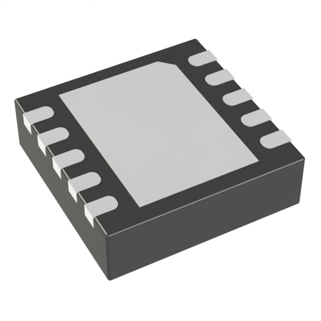
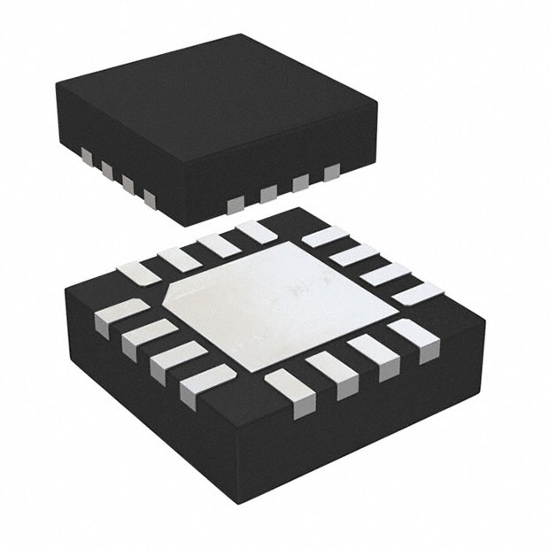
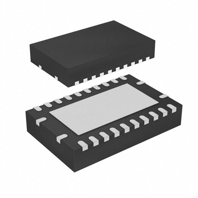
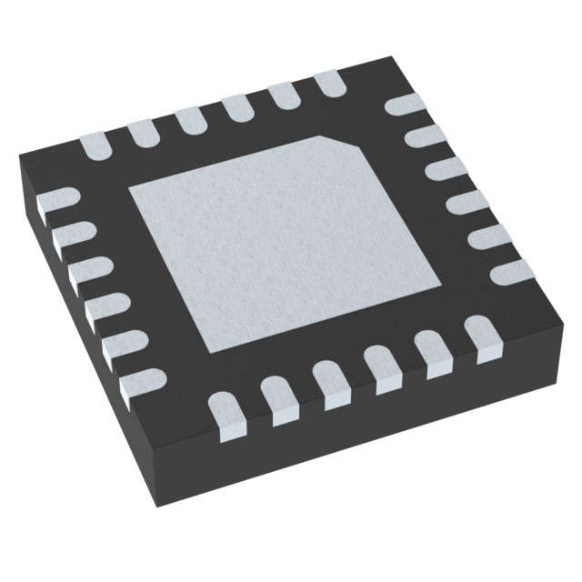
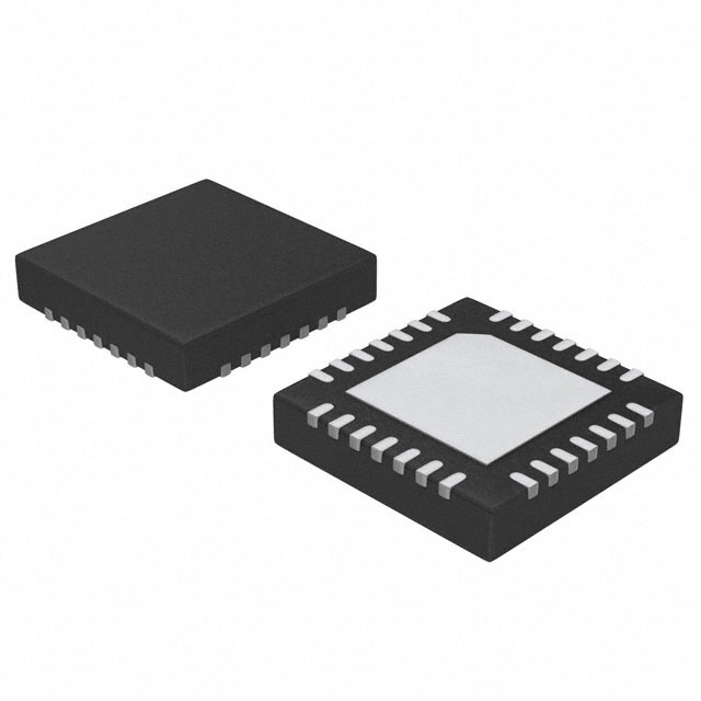
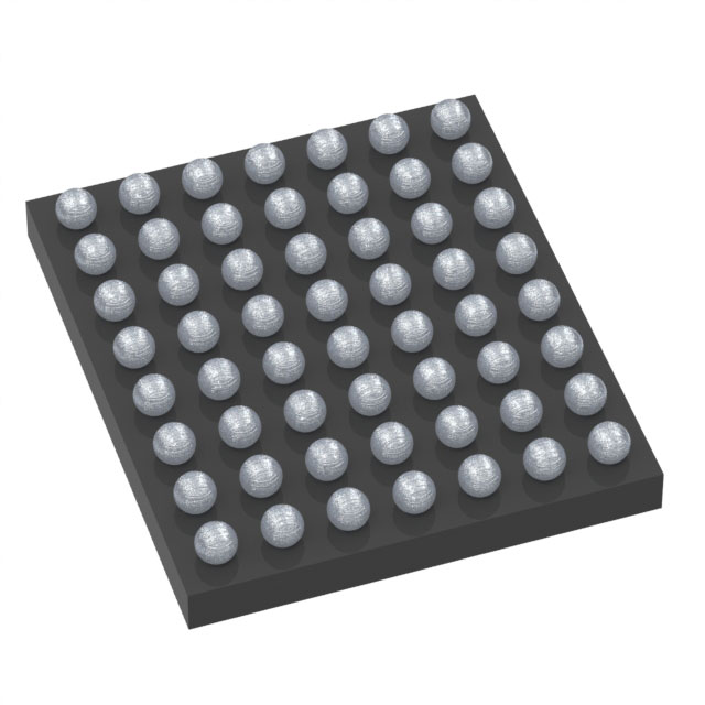
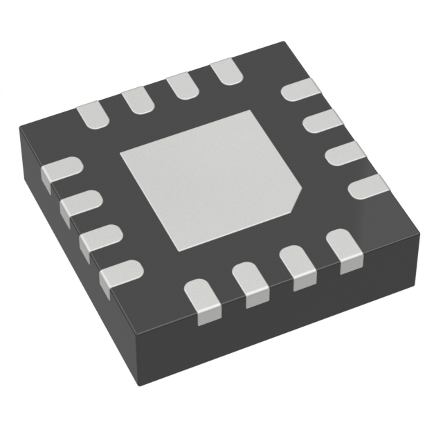
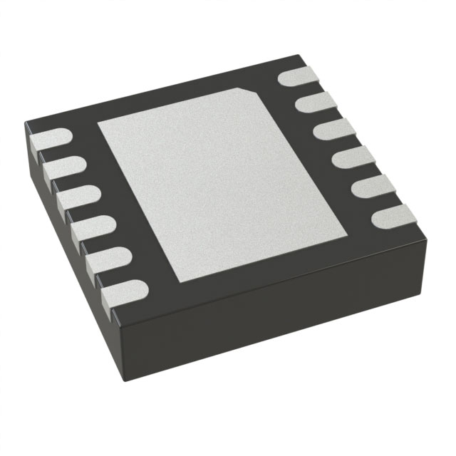
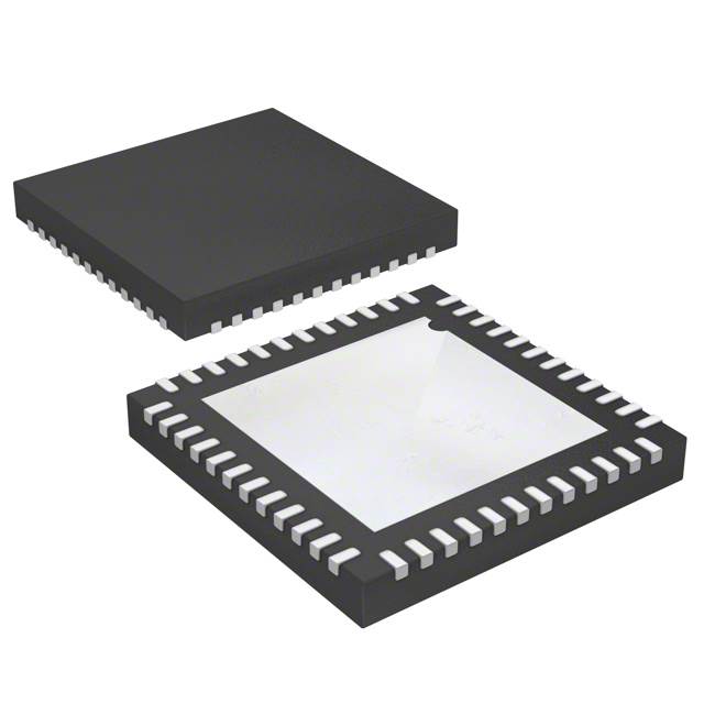
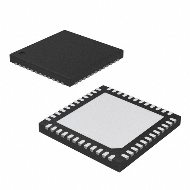
| Package | 32-pin FC2QFN (4mm × 4mm × 0.55mm) |
| Temperature Range | -40°C to +85°C |
| Max Charging Current | 5.5A (MAX77986 variant) |
| Max Input Voltage | 19V operating, 28V absolute maximum |
| Reverse Boost Power | Up to 18W |
2. Key Features
Charging Performance
- Fast Charging: Up to 5.5A programmable charge current (100mA to 5500mA in 50mA steps)
- High Efficiency: 92% buck efficiency at 4A/12V input, 92% charging efficiency at 3.5A/9V
- Wide Input Range: 4.7V to 19V operating, +28V absolute maximum rating
- Battery Support: Li-ion, Li-polymer, LiFePO4 chemistries
- Termination Voltage: Programmable 4.15V to 4.5375V (A variant) or 3.5V to 4.275V (B variant)
Smart Power Selector™
- Seamless power distribution between adapter, battery, and system
- Supplemental mode: Battery provides extra current when adapter is insufficient
- System can start with dead, missing, or deeply discharged battery
- True battery disconnect FET (RDSON = 7.7mΩ)
Reverse Boost (OTG)
- Programmable output voltage: 5V to 12V (100mV steps)
- Max output current: 3.1A (clamped at 18W power limit)
- True load disconnect in boost mode
- Programmable output current protection
Protection & Safety
- JEITA-compliant temperature-based charging
- Thermal regulation and thermal shutdown (155°C threshold)
- Input overvoltage (19.5V), undervoltage, and current limiting
- Battery overcurrent protection (3A to 10A programmable)
- Charge safety timer (3-8 hours programmable)
- Short-circuit protection
Advanced Features
- Spread spectrum modulation (±4%, ±8%, ±16%) for EMI reduction
- Fast unplug detection for 5V, 9V, and 15V sources
- I²C programmable interface (1MHz standard/fast mode, up to 3.4MHz HS-mode)
- Factory ship mode for minimal battery leakage
- Differential remote voltage sensing (BATSP/BATSN)
3. Electrical Specifications
3.1 Absolute Maximum Ratings
| Parameter | Symbol | Min | Max | Unit |
|---|---|---|---|---|
| CHGIN to PGND | VCHGIN | -0.3 | +28 | V |
| BYP to PGND | VBYP | -0.3 | +28 | V |
| SYS to AGND | VSYS | -0.3 | +6.0 | V |
| BATT to AGND | VBATT | -0.3 | +6.0 | V |
| BATT Continuous Current | IBATT | - | 10.0 | A (RMS) |
| LX Continuous Current | ILX | - | 9.8 | A (RMS) |
| Operating Temperature | TA | -40 | +85 | °C |
| Junction Temperature | TJ | - | +150 | °C |
| Storage Temperature | Tstg | -65 | +150 | °C |
3.2 Recommended Operating Conditions
| Parameter | Conditions | Min | Typ | Max | Unit |
|---|---|---|---|---|---|
| Input Voltage | - | 4.7 | - | 19 | V |
| System Voltage | - | 2.8 | 3.8 | 5.2 | V |
| Battery Voltage | - | 2.5 | 3.8 | 4.5 | V |
| I²C Supply (VIO) | - | 1.62 | 1.8 | 5.5 | V |
3.3 Key Electrical Characteristics
Input Current Limit (MAX77986)
- Range: 0.1A to 5.5A (50mA steps)
- Default: 500mA
- Accuracy: -3.5% to +3.5% (≥500mA, -5°C to +85°C)
- Charge Current
- Precharge: 40-80mA
- Trickle: 270-330mA (when TKEN=1)
- Fast Charge: 0.1A to 5.5A programmable
- Top-off: 150-850mA programmable
- Switching Frequency
- Selectable: 1.3MHz or 2.6MHz
- Inductor: 1.0μH for 1.3MHz, 0.47μH for 2.6MHz
- Thermal Regulation
- Programmable threshold: +85°C to +130°C (5°C steps)
- Default: +115°C
- Gain: -315mA/°C (reduces current by 5.73% per °C above threshold)
4. Pin Configuration and Functions
4.1 Package Outline (32-Pin FC2QFN)
Copy
TOP VIEW (Bumpside Down)
       ╔════════════════════════════╗
       ║  1  2  3  4  5  6  7  8  ║
       ║  9 10 11 12 13 14 15 16  ║
       ║ 17 18 19 20 21 22 23 24  ║
       ║ 25 26 27 28 29 30 31 32  ║
       ╚════════════════════════════╝
4.2 Pin Descriptions
| Pin | Name | Function | Type |
|---|---|---|---|
| 1 | DISQBAT | Disable internal QBATT FET (active-high) | Digital Input |
| 2 | THM | Thermistor connection for battery temperature monitoring | Analog |
| 3 | VDD | 1.8V LDO output for analog circuitry (bypass with 1μF) | Power Output |
| 4 | BATSN | Battery negative differential sense (Kelvin connection) | Analog Input |
| 5 | BATSP | Battery positive differential sense (Kelvin connection) | Analog Input |
| 6-8 | BATT | Battery positive terminal connection (bypass with 2×10μF) | Power |
| 9-11 | SYS | System output (bypass with 2×22μF, min 12μF effective) | Power |
| 12 | PVDD | 1.8V LDO for internal power (bypass with 1μF) | Power Output |
| 13 | DGND | Digital ground | Ground |
| 14-16 | PGND | Power ground | Ground |
| 17-19 | LX | Switching node (connect inductor between LX and SYS) | Power |
| 20 | BST | High-side FET driver supply (bypass 100nF to LX) | Analog |
| 21 | BYP | Input bypass/output for boost mode (bypass 2×22μF + 100nF) | Power |
| 22-23 | CHGIN | Charger input (bypass 2.2μF) | Power |
| 24 | SCL | I²C clock input | Digital Input |
| 25 | SDA | I²C data I/O | Digital I/O |
| 26 | EXTSM | Exit ship mode push-button input (active-high) | Digital Input |
| 27 | VIO | I²C supply voltage (bypass 1μF) | Power |
| 28 | AGND | Analog ground | Ground |
| 29 | STAT/QBEXT | LED status output or external QBATT control (configurable) | Digital Output |
| 30 | IRQB | Interrupt output (open-drain, pull-up required) | Digital Output |
| 31 | SUSPND | Suspend mode input (active-high) | Digital Input |
5. Functional Description
5.1 Smart Power Selector Operation
The IC manages power flow between CHGIN, BYP, SYS, and BATT through integrated switches:
- QCHGIN: Input switch with current limiting
- QHS/QLS: DC-DC converter switches (buck/boost)
- QBATT: Battery-to-system switch with overcurrent protection
- Power Priority (with valid adapter):
- Energy delivery to BYP (highest)
- Energy delivery to SYS (second)
- Battery charging (remaining capacity)
- Power Priority (battery only):
- Battery supplies SYS and BYP (if boost enabled)
5.2 Charging States
- No Input Power/Idle: Charger off, system powered by battery
- Precharge: VBATT < 2.5V, 40-80mA current
- Trickle Charge: 2.5V ≤ VBATT < 3.1V, 270-330mA (if TKEN=1)
- Fast-Charge CC: Constant current, max 5.5A
- Fast-Charge CV: Constant voltage at VBATTREG
- Top-off: Current < ITO for tTERM
- Done: Charging complete, 0mA current
- Timer Fault: Safety timeout (tPQ or tFC exceeded)
- Thermal Shutdown: TJ > 155°C
5.3 Reverse Boost (OTG) Mode
- MODE = 0x0A: Boost converter active, regulates VBYP to VBYPSET (5V-12V)
- QCHGIN Closed: Allows current sourcing from CHGIN up to OTG_ILIM limit
- Power Ceiling: 18W maximum (MAX77986)
- Protection: Overcurrent fault latch with optional auto-retry
5.4 Battery Overcurrent Protection
- Threshold: Programmable 3.0A to 10.0A (0.5A steps) via B2SOVRC[3:0]
- Response Time: 105μs (fast) or 10ms (delayed) debounce
- Action: Opens QBATT, shuts down buck, generates interrupt
- Retry: Auto-retry after 150ms if RECYCLE_EN=1
6. I²C Interface and Register Map
6.1 I²C Slave Address
- 7-bit: 0x6B (1101011b)
- Write: 0xD6
- Read: 0xD7
6.2 Key Configuration Registers
| Address | Register | Function | Default |
|---|---|---|---|
| 0x16 | CHG_CNFG_00 | Mode, spread spectrum, battery removal mask | 0x04 |
| 0x17 | CHG_CNFG_01 | Trickle enable, watchdog, fast-charge timer | 0x52 |
| 0x18 | CHG_CNFG_02 | Fast-charge current (CHG_CC) | 0x09 (450mA) |
| 0x1A | CHG_CNFG_04 | Min SYS voltage, termination voltage | 0x24 (4.2V) |
| 0x1B | CHG_CNFG_05 | Battery overcurrent protection | 0x46 (5.5A) |
| 0x1F | CHG_CNFG_09 | Input current limit (CHGIN_ILIM) | 0x09 (500mA) |
| 0x20 | CHG_CNFG_10 | OTG current limit, recycle enable | 0x40 (500mA) |
| 0x21 | CHG_CNFG_11 | BYP output voltage (VBYPSET) | 0x01 (5.1V) |
| 0x23 | CHG_CNFG_13 | JEITA enable, thermal regulation temp | 0x46 (115°C) Register Protection: Critical registers (0x17-0x1E) are write-protected by CHGPROT bits (0x1C). Write 0x11 to CHG_CNFG_06[3:2] to unlock. |
7. Typical Application Circuit and Layout
7.1 Application Schematic
CHGIN ── 2.2μF ── PGND
   │
BYP ── 2×22μF + 100nF ── PGND
   │
LX ←── Inductor (1μH @ 1.3MHz) ── SYS ── 2×22μF ── PGND
   │
BATT ── 2×10μF ── PGND
   │
BATSP/BATSN → Kelvin sense to battery terminals
   │
THM ── NTC Thermistor ── AGND
   │
VDD ── 1μF ── AGND
PVDD ── 1μF ── PGND
VIO ── 1μF ── AGND
7.2 Critical Layout Guidelines
- Ground Separation: Keep AGND/DGND isolated from PGND; connect at single point near input capacitor
- Bypass Capacitors: Place CHGIN, BYP, SYS, and BATT capacitors as close as possible to IC pins
- High Current Paths: Use wide, short traces for CHGIN, BYP, SYS, BATT, LX, and PGND
- Kelvin Sensing: Route BATSP/BATSN directly to battery terminals; avoid vias and shared traces
- Thermal Design: Use exposed pad connection to PGND plane for heat dissipation
- Inductor Placement: Minimize LX trace length to reduce EMI
8. Ordering Informatio
| Part Number | Temp Range | Max Charge Current | Battery Type | Package | Default Mode |
|---|---|---|---|---|---|
| MAX77986AEFD+ | -40°C to +85°C | 5.5A | General Li-ion | 32-FC2QFN | 0x04 |
| MAX77986AEFD+T | -40°C to +85°C | 5.5A | General Li-ion | 32-FC2QFN (Tape/Reel) | 0x04 |
| MAX77986BEFD+ | -40°C to +85°C | 5.5A | LiFePO4 | 32-FC2QFN | 0x04 |
| MAX77986BEFD+T | -40°C to +85°C | 5.5A | LiFePO4 | 32-FC2QFN (Tape/Reel) | 0x04 Package Code: EFD = 32-pin FC2QFN 4mm × 4mm + Suffix: Lead(Pb)-free/RoHS compliant T Suffix: Tape and reel packaging Note: The "D" in "DEFD+" is not explicitly defined in the current revision of the datasheet. The part numbers are designated as AEFD+ (General Li-ion) and BEFD+ (LiFePO4). Please confirm exact part number with Analog Devices. |
9. Document Information
- Datasheet Revision: 3 (February 2025)
- Document Number: 19-101295
- For Chip Revision: PASS2 (0b010) - Contact Analog Devices for PASS1 (0b001) details
- CHIP_ID Register: 0x86 for MAX77986
- CHIP_REVISION Register: 0xA (A variant) or 0xB (B variant)
Purchase
No need to register to order from JMBom Electronics, but signing in lets you track your order like a pro. Give it a try for a smoother shopping ride.
Means
Easy peasy! Pay your way with PayPal, Credit Card, or wire transfer in USD. We've got you covered.
RFQ(Request for Quotations)
Get the freshest prices and stock updates by asking for a quote! Our sales team will shoot you an email within a day. It's that simple.
IMPORTANT NOTICE
1. Look out for your order details in your inbox! (If it's missing, check the spam folder just in case.)
2. Our sales manager will double-check the order and keep you posted on any price or stock changes. No worries, we've got you covered.

Shipping Rate
We ship orders once a day around 5 p.m., except Sunday. Once shipped, the estimated delivery time depends on the courier company you choose, usually 5-7 working days.

Shipping Methods
We provide DHL, FedEx, UPS, EMS, SF Express, and Registered Air Mail international shipping.


Payment
You can pay the orders on the website directly or pay by wire transfer offline. We support: Paypal、VISA、Credit Card.


Analog Devices Inc.(ADI)
Analog Devices Inc.(ADI)
Analog Devices Inc.(ADI)
Analog Devices Inc.(ADI)
Analog Devices Inc.(ADI)
Analog Devices Inc.(ADI)
Analog Devices Inc.(ADI)
Analog Devices Inc.(ADI)
Analog Devices Inc.(ADI)
Analog Devices Inc.(ADI)
Analog Devices Inc.(ADI)
Analog Devices Inc.(ADI)