NXP SSTUH32866EC/G,551


- Part Number:
SSTUH32866EC/G,551
- Manufacturer:
- Category:
- RoHs:
 RoHS Compliant
 - Datasheet:
 SSTUH32866EC/G,551_Datesheet
 - Description:
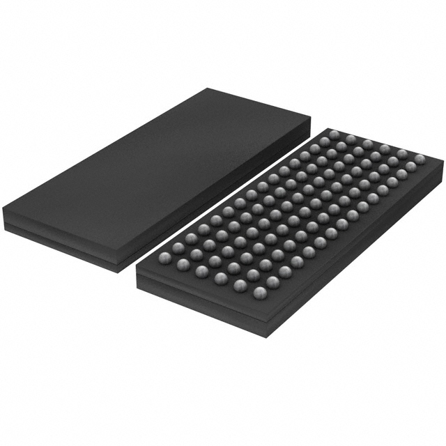
IC BUFFER 1.8V 25BIT SOT536-1
- In stock 0

DESCRIPTION
· The SSTUH32866 is a 1.8 V configurable register designed for DDR2 memory modules with parity checking.
· It complies with the JEDEC JESD82-7 standard and adds a parity checking function.
· Configurable to 25-bit 1:1 or 14-bit 1:2 topologies, designated as Register A or B on DIMM.
· Accepts a parity bit from the memory controller, compares it with DIMM-independent data inputs, and indicates parity errors on the QERR pin.
· Packaged in a 96-ball LFBGA package (13.5 mm × 5.5 mm).
· Identical to SSTU32866 in function and performance, with higher-drive outputs for heavy load nets.
FEATURES
· Configurable register for DDR2 Registered DIMM applications.
· Higher output drive strength optimized for high-capacitive load nets.
· Configurable to 25-bit 1:1 or 14-bit 1:2 mode.
· Controlled output impedance drivers for optimal signal integrity and speed.
· Exceeds JESD82-7 speed performance (1.8 ns max. single-bit switching propagation delay; 2.0 ns max. mass-switching).
· Supports up to 450 MHz clock frequency.
· Optimized pinout for high-density DDR2 module design.
· Chip-selects minimize power consumption by gating data outputs.
· Supports SSTL_18 data inputs.
· Checks parity on DIMM-independent data inputs.
· Partial parity output and input allow cascading of two SSTUH32866s for correct parity error processing.
· Differential clock (CK and CK) inputs.
APPLICATIONS
· DDR2 Registered DIMM applications.
· High-capacitive load nets, such as stacked DRAMs.
· High-density DDR2 module designs.
Purchase
No need to register to order from JMBom Electronics, but signing in lets you track your order like a pro. Give it a try for a smoother shopping ride.
Means
Easy peasy! Pay your way with PayPal, Credit Card, or wire transfer in USD. We've got you covered.
RFQ(Request for Quotations)
Get the freshest prices and stock updates by asking for a quote! Our sales team will shoot you an email within a day. It's that simple.
IMPORTANT NOTICE
1. Look out for your order details in your inbox! (If it's missing, check the spam folder just in case.)
2. Our sales manager will double-check the order and keep you posted on any price or stock changes. No worries, we've got you covered.

Shipping Rate
We ship orders once a day around 5 p.m., except Sunday. Once shipped, the estimated delivery time depends on the courier company you choose, usually 5-7 working days.

Shipping Methods
We provide DHL, FedEx, UPS, EMS, SF Express, and Registered Air Mail international shipping.


Payment
You can pay the orders on the website directly or pay by wire transfer offline. We support: Paypal、VISA、Credit Card.