


ADXL343: High-Performance 3-Axis MEMS Accelerometer
Catalog
OverviewKey FeaturesTypical ApplicationsADXL343 BLOCK DIAGRAMAbsolute Maximum RatingsPIN CONFIGURATION AND FUNCTION DESCRIPTIONSTheory of OperationPower SequencingSERIAL COMMUNICATIONSSPI Digital Input/Output SpecificationsI²C Serial CommunicationsInterruptsConclusionOverview
The ADXL343 is a flexible 3-axis digital MEMS accelerometer designed for low-g measurements. Its selectable measurement range and bandwidth, combined with configurable built-in motion detection, make it ideal for monitoring acceleration in a wide range of applications. The device can withstand shocks up to 10,000 g and operates reliably across a wide temperature range (−40°C to +85°C), making it suitable even in demanding environments.
ADXL343
The ADXL343 offers high-resolution acceleration measurements (13-bit) with a range of up to ±16 g. Data is output in 16-bit two’s complement format and can be accessed through either a 3- or 4-wire SPI interface or an I²C interface. It can detect static acceleration, such as gravity for tilt sensing, as well as dynamic acceleration caused by movement or impact. With a resolution of 3.9 mg/LSB, it can measure inclination changes smaller than 1°.
The accelerometer includes advanced sensing features. Activity and inactivity detection monitor motion or the lack of it. Tap detection can identify single or double taps in any direction, while free-fall detection senses if the device is falling. These events can be routed to either of the two interrupt pins independently.
An integrated FIFO buffer with 32 levels helps manage data efficiently, reducing the workload on the host processor and lowering overall system power consumption.
The ADXL343 comes in a compact, thin 14-terminal plastic package measuring just 3 mm × 5 mm × 1 mm.
Key Features
- Versatile accelerometer with 10- to 13-bit resolution, suitable for a wide range of applications
- Digital output via SPI (3- or 4-wire) and I²C interfaces
- Built-in motion detection enables easy tap, double-tap, activity, inactivity, and free-fall sensing
- User-configurable thresholds for customized operation
- Interrupts can be independently assigned to two interrupt pins
- Low-power operation down to 23 µA, with embedded FIFO to minimize system power consumption
- Wide supply voltage range: 2.0 V to 3.6 V
- I/O voltage range: 1.7 V to VS
- Operates reliably across a broad temperature range (−40°C to +85°C)
- Can survive shocks up to 10,000 g
- Compact, thin, lead-free, RoHS-compliant 3 mm × 5 mm × 1 mm LGA package
Typical Applications
- Mobile handsets and tablets
- Gaming controllers and pointing devices
- Hard disk drive (HDD) protection systems
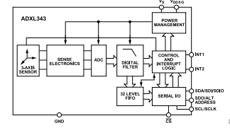
ADXL343 BLOCK DIAGRAM
Specifications
Conditions: TA = 25°C, VS = 2.5 V, VDD I/O = 1.8 V, acceleration = 0 g, CS = 10 µF tantalum, CI/O = 0.1 µF, output data rate (ODR) = 800 Hz unless otherwise noted. All minimum and maximum values are guaranteed; typical values are for reference only.
Sensor Input (Each Axis)
- Measurement Range: User-selectable ±2, ±4, ±8, ±16 g
- Nonlinearity: ±0.5% of full scale
- Inter-Axis Alignment Error: ±0.1°
- Cross-Axis Sensitivity: ±1%
Output Resolution (Each Axis)
- ±2 g Range: 10-bit
- ±4 g Range: 11-bit
- ±8 g Range: 12-bit
- ±16 g Range: 13-bit
Sensitivity (Each Axis)
- XOUT, YOUT, ZOUT Full Resolution: 256 LSB/g
- ±2 g, 10-bit: 256 LSB/g
- ±4 g, 10-bit: 128 LSB/g
- ±8 g, 10-bit: 64 LSB/g
- ±16 g, 10-bit: 32 LSB/g
- Deviation from Ideal: ±1%
- Scale Factor Full Resolution: 3.9 mg/LSB (varies with range: ±4 g = 7.8 mg/LSB, ±8 g = 15.6 mg/LSB, ±16 g = 31.2 mg/LSB)
- Temperature Sensitivity Change: ±0.01 %/°C
0 g Offset (Each Axis)
- Output Deviation from Ideal: ±35 mg
- Offset vs Temperature: ±0.8 mg/°C
Noise
- X, Y, Z axes, ODR = 100 Hz, ±2 g, 10-bit or full range: 1.1 LSB rms
Output Data Rate & Bandwidth
- ODR: 0.1 Hz to 3200 Hz (user-selectable)
Self-Test
- X-axis Output Change: 0.20 to 2.10 g
- Y-axis Output Change: −2.10 to −0.20 g
- Z-axis Output Change: 0.30 to 3.40 g
Power Supply
- Operating Voltage (VS): 2.0 – 3.6 V
- Interface Voltage (VDD I/O): 1.7 – VS V
- Supply Current: ODR ≥ 100 Hz → 140 µA; ODR < 10 Hz → 30 µA
- Standby Mode Leakage Current: 0.1 µA
Additional Specifications
- Turn-On and Wake-Up Time: ODR = 3200 Hz → 1.4 ms (depends on user-selected bandwidth; e.g., at 100 Hz ODR, ~11.1 ms; for other data rates, ~τ + 1.1 ms, where τ = 1 / data rate)
- Operating Temperature Range: −40°C to +85°C
- Device Weight: 30 mg
Notes:
- Typical specifications represent at least 68% of devices and are based on worst-case mean ±1σ, except 0 g output and sensitivity, which are target values. Deviations from ideal indicate worst-case mean ±1σ.
- Cross-axis sensitivity refers to the coupling effect between any two axes.
- Bandwidth is defined as the −3 dB frequency and equals half the output data rate (bandwidth = ODR/2).
- Output format differs for 3200 Hz and 1600 Hz ODRs compared to other rates (see “Data Formatting of Upper Data Rates” section).
- Data rates below 6.25 Hz may show additional offset shifts with temperature (see “Offset Performance at Lowest Data Rates” section).
- Self-test output change = output (g) with SELF_TEST bit = 1 minus output with SELF_TEST bit = 0. Device reaches final value after 4 × τ (τ = 1 / data rate). Must be in normal power mode (LOW_POWER bit = 0) for proper self-test operation.
- Turn-on and wake-up times depend on the selected bandwidth, as described above.
Absolute Maximum Ratings
| Parameter | Rating |
|---|---|
| Acceleration | Any axis, unpowered: 10,000 g Any axis, powered: 10,000 g |
| Supply Voltage (VS) | −0.3 V to +3.9 V |
| Interface Voltage (VDD I/O) | −0.3 V to +3.9 V |
| Digital Pins | −0.3 V to VDD I/O + 0.3 V, or 3.9 V (whichever is lower) |
| All Other Pins | −0.3 V to +3.9 V |
| Output Short-Circuit (any pin to ground) | Indefinite |
| Temperature Range | Powered: −40°C to +105°C Storage: −40°C to +105°C |
Caution: Exceeding these limits may cause permanent damage. These are stress ratings only; operation beyond the recommended limits is not guaranteed and may affect long-term reliability.
Thermal Resistance
| Package Type | θJA (Junction-to-Ambient) | θJC (Junction-to-Case) | Device Weight |
|---|---|---|---|
| 14-Terminal LGA | 150°C/W | 85°C/W | 30 mg |
Recommended Soldering Profile
Based on JEDEC Standard J-STD-020D.1. Follow solder paste manufacturer recommendations for best results.
| Profile Feature | Sn63/Pb37 | Pb-Free |
|---|---|---|
| Average Ramp Rate (TL → TP) | 3°C/sec max | 3°C/sec max |
| Preheat Minimum Temperature (TSMIN) | 100°C | 150°C |
| Preheat Maximum Temperature (TSMAX) | 150°C | 200°C |
| Time from TSMIN to TSMAX (tS) | 60–120 sec | 60–180 sec |
| Ramp-Up Rate (TSMAX → TL) | 3°C/sec max | 3°C/sec max |
| Liquid Temperature (TL) | 183°C | 217°C |
| Time Above TL (tL) | 60–150 sec | 60–150 sec |
| Peak Temperature (TP) | 240 +0/−5°C | 260 +0/−5°C |
| Time at TP − 5°C (tP) | 10–30 sec | 20–40 sec |
| Ramp-Down Rate | 6°C/sec max | 6°C/sec max |
| Time from 25°C to Peak Temperature | ≤6 minutes | ≤8 minutes |
ESD Caution
This device is sensitive to electrostatic discharge (ESD). Charged devices and circuit boards can discharge without warning. Although the device includes proprietary or patented protection circuitry, exposure to high-energy ESD may still cause damage. Proper ESD precautions must be observed to prevent performance degradation or loss of functionality.
PIN CONFIGURATION AND FUNCTION DESCRIPTIONS
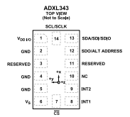
Pin Configuration (Top View)
Pin Function Descriptions
| Pin No. | Mnemonic | Description |
|---|---|---|
| 1 | VDD I/O | Digital interface supply voltage. |
| 2 | GND | Connect to ground. |
| 3 | RESERVED | Reserved; connect to VS or leave open. |
| 4 | GND | Connect to ground. |
| 5 | GND | Connect to ground. |
| 6 | VS | Supply voltage. |
| 7 | CS | Chip Select input. |
| 8 | INT1 | Interrupt 1 output. |
| 9 | INT2 | Interrupt 2 output. |
| 10 | NC | Not internally connected. |
| 11 | RESERVED | Reserved; connect to ground or leave open. |
| 12 | SDO / ALT ADDRESS | SPI 4-wire Serial Data Output / I²C alternate address select. |
| 13 | SDA / SDI / SDIO | I²C Serial Data / SPI 4-wire Serial Data Input / SPI 3-wire Serial Data Input & Output. |
| 14 | SCL / SCLK | Clock input: SCL for I²C, SCLK for SPI. |
Theory of Operation
The ADXL343 is a fully integrated 3-axis accelerometer with selectable measurement ranges of ±2 g, ±4 g, ±8 g, or ±16 g. It can detect both dynamic acceleration caused by motion or shock and static acceleration, such as gravity, making it suitable for tilt-sensing applications.
The sensor consists of a polysilicon surface-micromachined structure built on a silicon wafer. Polysilicon springs suspend the structure above the wafer, providing resistance against forces generated by acceleration.
Acceleration causes the structure (proof mass) to deflect. This deflection is measured using differential capacitors, which include fixed plates and plates attached to the moving mass. When acceleration occurs, the proof mass shifts, unbalancing the differential capacitor and producing an output signal proportional to the acceleration. Phase-sensitive demodulation is used to determine both the magnitude and direction of the acceleration.
Power Sequencing
Power may be applied to VS and VDD I/O in any order without damaging the device. The interface voltage level is determined by VDD I/O, which must be present to prevent bus conflicts.
- Single-Supply Operation: VDD I/O can be the same as the main supply voltage (VS).
- Dual-Supply Operation: VDD I/O can differ from VS to match the required interface voltage, provided VS ≥ VDD I/O.
Once VS is applied, the device enters standby mode, minimizing power consumption while waiting for VDD I/O and the command to enter measurement mode. Measurement mode is activated by setting the measure bit (D3) in the POWER_CTL register (0x2D).
While in standby mode, all registers can be read or written to configure the device. It is recommended to complete configuration in standby mode before enabling measurement. Clearing the measure bit returns the device to standby mode.
Power Sequencing
| Condition | VS | VDD I/O | Description |
|---|---|---|---|
| Power Off | Off | Off | Device is completely powered down. Communication bus conflict may occur. |
| Bus Disabled | On | Off | Device is in standby mode, but communication is unavailable and may conflict with the bus. Minimize the duration of this state during power-up. |
| Bus Enabled | Off | On | No sensor functions are active, but no communication bus conflict occurs. |
| Standby or Measurement | On | On | At power-up, the device enters standby mode, waiting for the command to start measurement. Once measurement mode is enabled, all sensor functions become active. |
Power Savings
The ADXL343 dynamically adjusts its power consumption based on the selected output data rate (ODR). For further energy efficiency, a low-power mode is available. In this mode, the internal sampling rate is reduced, lowering power consumption for ODRs between 12.5 Hz and 400 Hz, though with a slight increase in noise. To enable low-power mode, set the LOW_POWER bit (Bit 4) in the BW_RATE register (0x2C). Only the data rates listed in the low-power table benefit from this mode; using other rates provides no advantage over normal operation. All current consumption values assume VS = 2.5 V.
Typical Current Consumption vs. Data Rate (Normal Mode, TA = 25°C, VS = 2.5 V, VDD I/O = 1.8 V)
| ODR (Hz) | Bandwidth (Hz) | Rate Code | IDD (µA) |
|---|---|---|---|
| 3200 | 1600 | 1111 | 140 |
| 1600 | 800 | 1110 | 90 |
| 800 | 400 | 1101 | 140 |
| 400 | 200 | 1100 | 140 |
| 200 | 100 | 1011 | 140 |
| 100 | 50 | 1010 | 140 |
| 50 | 25 | 1001 | 90 |
| 25 | 12.5 | 1000 | 60 |
| 12.5 | 6.25 | 0111 | 50 |
| 6.25 | 3.13 | 0110 | 45 |
| 3.13 | 1.56 | 0101 | 40 |
| 1.56 | 0.78 | 0100 | 34 |
| 0.78 | 0.39 | 0011 | 23 |
| 0.39 | 0.20 | 0010 | 23 |
| 0.20 | 0.10 | 0001 | 23 |
| 0.10 | 0.05 | 0000 | 23 |
Typical Current Consumption vs. Data Rate (Low-Power Mode, TA = 25°C, VS = 2.5 V, VDD I/O = 1.8 V)
| ODR (Hz) | Bandwidth (Hz) | Rate Code | IDD (µA) |
|---|---|---|---|
| 400 | 200 | 1100 | 90 |
| 200 | 100 | 1011 | 60 |
| 100 | 50 | 1010 | 50 |
| 50 | 25 | 1001 | 45 |
| 25 | 12.5 | 1000 | 40 |
| 12.5 | 6.25 | 0111 | 34 |
Auto Sleep Mode
The device can further reduce power by automatically entering sleep mode during periods of inactivity. To enable this feature:
- Set THRESH_INACT (0x25) and TIME_INACT (0x26) to define inactivity.
- Set AUTO_SLEEP (Bit D4) and the link bit (Bit D5) in POWER_CTL (0x2D).
At ODRs below 12.5 Hz used in auto-sleep mode, typical current consumption is 23 µA (VS = 2.5 V).
Standby Mode
For the lowest power consumption, use standby mode, where current drops to 0.1 µA (typical). No measurements are taken in standby. Enter standby by clearing the measure bit (Bit D3) in POWER_CTL (0x2D). FIFO contents are preserved in this mode.
Serial Communications
The ADXL343 supports both I²C and SPI digital interfaces and operates as a slave in either mode.
- I²C Mode: Enabled when the CS pin is tied high to VDD I/O. The CS pin must always be either tied high to VDD I/O or driven by an external controller, as leaving it unconnected prevents communication with the device.
- SPI Mode: The CS pin is controlled by the bus master. During writes to the ADXL343, any data sent from the device to the master should be ignored in both SPI and I²C modes.
SPI Configuration
- Supports 3-wire or 4-wire SPI configurations.
- The SPI bit (Bit D6) in the DATA_FORMAT register (0x31) selects the mode: clearing the bit selects 4-wire SPI, setting the bit selects 3-wire SPI.
- Maximum SPI clock speed is 5 MHz with 100 pF maximum load.
- Timing follows clock polarity (CPOL) = 1 and clock phase (CPHA) = 1.
- If power is applied before configuring the host processor’s clock polarity and phase, ensure the CS pin is high before changing these settings.
- For 3-wire SPI, it is recommended to pull the SDO pin either up to VDD I/O or down to GND via a 10 kΩ resistor.
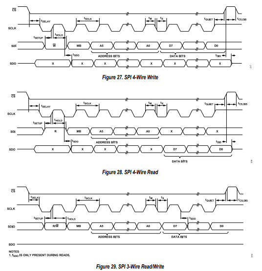
SPI Communication Details
- The CS pin is the serial port enable line and is controlled by the SPI master. It must go low at the start of a transmission and high at the end.
- SCLK is the serial clock provided by the SPI master and should idle high when no transmission occurs.
- SDI and SDO are the serial data input and output, respectively. Data is updated on the falling edge of SCLK and should be sampled on the rising edge.
Multi-Byte Transfers
- To read or write multiple consecutive bytes in a single SPI transaction, set the multiple-byte (MB) bit, located after the R/W bit in the first byte.
- After sending the register address and first data byte, each subsequent set of eight clock pulses advances the register pointer to the next address.
- This continues until CS goes high.
- To access non-sequential registers, CS must be deasserted between transmissions, and each new register must be addressed separately.
SPI Timing
- Refer to timing diagrams for 3-wire and 4-wire SPI in the datasheet.
- Logic thresholds and timing parameters in Tables 9 and 10 must always be met for correct operation.
- Recommended SPI speeds relative to output data rate: 3200 Hz and 1600 Hz ODR: ≥ 2 MHz 800 Hz ODR: ≥ 400 kHz Other rates: scale proportionally (e.g., 200 Hz ODR → ≥ 100 kHz)
- Using output data rates above recommended SPI speeds may cause missing samples or increased noise.
Preventing Bus Traffic Errors
- The CS pin also enables I²C mode. On a SPI bus with multiple devices, CS is held high when communicating with other devices.
- If another SPI device transmits a command that resembles an I²C start condition, the ADXL343 may mistakenly interpret it as an I²C command, potentially interfering with bus traffic.
- To prevent this, it is recommended to place a logic gate on the SDI pin (as shown in Figure 26), which holds the SDA line high when CS is high.
- This precaution is only necessary when the ADXL343 shares a SPI bus with multiple devices.
SERIAL COMMUNICATIONS
SPI Digital Input/Output Specifications
Digital Input
- Low-Level Input Voltage (VIL): ≤ 0.3 × VDD I/O
- High-Level Input Voltage (VIH): ≥ 0.7 × VDD I/O
- Low-Level Input Current (IIL): 0.1 µA (at VIN = VDD I/O)
- High-Level Input Current (IIH): −0.1 µA (at VIN = 0 V)
Digital Output
- Low-Level Output Voltage (VOL): ≤ 0.2 × VDD I/O (at IOL = 10 mA)
- High-Level Output Voltage (VOH): ≥ 0.8 × VDD I/O (at IOH = −4 mA)
- Low-Level Output Current (IOL): 10 mA (at VOL = VOL, max)
- High-Level Output Current (IOH): −4 mA (at VOH = VOH, min)
Other Characteristics
- Pin Capacitance: 8 pF (fIN = 1 MHz, VIN = 2.5 V)
SPI Timing (TA = 25°C, VS = 2.5 V, VDD I/O = 1.8 V)
| Parameter | Min | Max | Unit | Description |
|---|---|---|---|---|
| fSCLK | — | 5 | MHz | SPI clock frequency |
| tSCLK | 200 | 1/(SPI clock) | ns | SCLK mark-space ratio: 40/60 to 60/40 |
| tDELAY | 5 | — | ns | CS falling edge to SCLK falling edge |
| tQUIET | 5 | — | ns | SCLK rising edge to CS rising edge |
| tDIS | 10 | — | ns | CS rising edge to SDO disabled |
| tCS,DIS | — | 150 | ns | Minimum CS deassertion between SPI transactions |
| tS | — | 0.3 × tSCLK | ns | SCLK low pulse width (space) |
| tM | — | 0.3 × tSCLK | ns | SCLK high pulse width (mark) |
| tSETUP | 5 | — | ns | SDI valid before SCLK rising edge |
| tHOLD | 5 | — | ns | SDI valid after SCLK rising edge |
| tSDO | — | 40 | ns | SCLK falling edge to SDO/SDIO output transition |
| tR | — | 20 | ns | SDO/SDIO output high-to-low transition |
| tF | — | 20 | ns | SDO/SDIO output low-to-high transition |
Notes:
- CS, SCLK, SDI, and SDO pins are not internally pulled; they must be actively driven.
- Timing limits are based on characterization at fSCLK = 5 MHz with a bus load capacitance of 100 pF; not production-tested.
- Timing values are measured with respect to VIL and VIH input thresholds (Table 9).
- Output rise and fall times are measured with a 150 pF capacitive load.
I²C Serial Communications
- The ADXL343 operates in I²C mode when the CS pin is tied high to VDD I/O, requiring only a simple 2-wire connection.
- The device follows the UM10204 I²C-Bus Specification and User Manual, Rev. 03 (19 June 2007) from NXP Semiconductor.
- Supported data rates: Standard mode: 100 kHz Fast mode: 400 kHz
- Communication must meet bus parameters specified in Tables 11 and 12.
- Both single- and multi-byte reads/writes are supported.
- I²C Addressing: ALT ADDRESS pin high: 7-bit address = 0x1D → write: 0x3A, read: 0x3B ALT ADDRESS pin low (GND): 7-bit address = 0x53 → write: 0xA6, read: 0xA7
- Unused pins have no internal pull-up or pull-down resistors. Both CS and ALT ADDRESS pins must be connected: CS → VDD I/O ALT ADDRESS → VDD I/O or GND
- Maximum Output Data Rate (ODR): For 400 kHz I²C: up to 800 Hz Scales linearly with I²C speed (e.g., 100 kHz I²C → max ODR = 200 Hz)
- Exceeding the recommended maximum ODR may cause missing samples or additional noise in acceleration data.
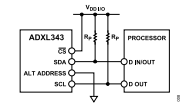
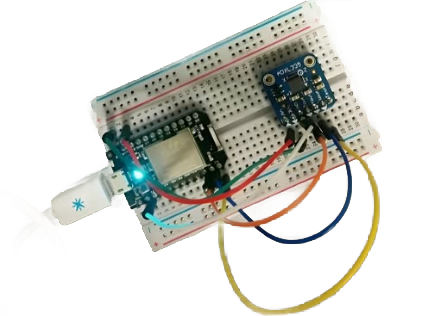
I2C Connection Diagram (Address 0x53)
I²C Bus Voltage and Pull-Up Requirements
- When sharing the I²C bus with other devices, the nominal operating voltage of any other device must not exceed VDD I/O by more than 0.3 V.
- External pull-up resistors (RP) are required for proper I²C operation.
- Refer to the UM10204 I²C-Bus Specification and User Manual, Rev. 03 (19 June 2007) when selecting pull-up resistor values to ensure reliable communication.
Interrupts
The ADXL343 provides two interrupt output pins: INT1 and INT2.
- Both pins are push-pull, low-impedance outputs.
- Default configuration: active high; can be changed to active low by setting the INT_INVERT bit in the DATA_FORMAT register (0x31).
- Multiple interrupt functions can be used simultaneously, although some functions may share pins.
Interrupt Configuration:
- Enable interrupts by setting the corresponding bit in the INT_ENABLE register (0x2E).
- Map interrupts to either INT1 or INT2 via the INT_MAP register (0x2F).
- Recommended procedure: Configure interrupt functions and mapping before enabling interrupts. To reconfigure, disable the interrupt first by clearing the corresponding bit in INT_ENABLE, then reconfigure and re-enable it. This prevents accidental interrupts during configuration.
Interrupt Clearing:
- Data-related interrupts: cleared by reading the data registers (0x32–0x37) until the condition is no longer valid.
- Other interrupts: cleared by reading the INT_SOURCE register (0x30).
Interrupt Pin Specifications (Table 13):
| Parameter | Test Conditions | Min | Max | Unit | Description |
|---|---|---|---|---|---|
| Low-Level Output Voltage (VOL) | IOL = 300 µA | — | 0.2 × VDD I/O | V | Digital output low voltage |
| High-Level Output Voltage (VOH) | IOH = −150 µA | 0.8 × VDD I/O | — | V | Digital output high voltage |
| Low-Level Output Current (IOL) | VOL = VOL,max | — | 300 | µA | Sink current capability |
| High-Level Output Current (IOH) | VOH = VOH,min | −150 | — | µA | Source current capability |
| Pin Capacitance | fIN = 1 MHz, VIN = 2.5 V | — | 8 | pF | Output pin capacitance |
| Rise Time (tR) | CLOAD = 150 pF | — | 210 | ns | VOL,max → VOH,min transition |
| Fall Time (tF) | CLOAD = 150 pF | — | 150 | ns | VOH,min → VOL,max transition |
Notes:
- Limits are based on characterization, not production tested.
- Rise and fall times measured with 150 pF load.
Conclusion
The ADXL343 is a high-performance, low-power, 3-axis MEMS accelerometer offering versatile measurement ranges (±2 g to ±16 g) and digital output via SPI or I²C interfaces. With built-in motion detection, tap, free-fall, and activity/inactivity sensing, it is suitable for a wide range of applications, including mobile devices, gaming peripherals, and HDD protection. Its robust design supports operation across a wide temperature range (−40°C to +85°C) and survives shocks up to 10,000 g. Low-power modes, FIFO memory, and configurable interrupts enable efficient system integration and optimized power management, making the ADXL343 a reliable solution for precise acceleration and tilt sensing in harsh environments.

Amanda Miller
Amanda Miller is a senior electronics engineer with 6 years of experience. She focuses on studying resistors, transistors, and package design in detail. Her deep knowledge helps her bring innovation and high standards to the electronics industry.
Subscribe to JMBom Electronics !


