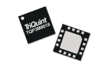
High-Performance TQP3M9018 LNA – Request Your Quote Today
Catalog
TQP3M9018 Product OverviewKey FeaturesApplicationsTQP3M9018 Package Marking and DimensionsTQP3M9018 Pad Configuration and DescriptionRecommended PCB Layout PatternTape and Reel Information – Reel DimensionsHandling PrecautionsBill of Materials – TQP3M9018-PCB_RF (500–4000 MHz)ConclusionContact us today for a TQP3M9018 quote!TQP3M9018 Product Overview
The TQP3M9018 is a high-linearity, cascade-capable gain block amplifier offered in a cost-effective surface-mount package. At 1.9 GHz, it typically delivers 20.5 dB of gain, an output IP3 of +37 dBm, and a low 1.3 dB noise figure, while consuming just 85 mA of current. The device comes in a lead-free, green, RoHS-compliant, industry-standard 16-pin 3x3 mm QFN package.
High-Performance TQP3M9018
The TQP3M9018 provides consistently high gain across a wide frequency range along with a very low noise figure. This makes it suitable for both transmitter and receiver signal chains in high-performance systems. Built on a high-performance E-pHEMT process, the amplifier is internally matched and requires only an external RF choke plus blocking or bypass capacitors to run from a single +5 V supply. Its integrated active bias circuit ensures stable performance over variations in bias and temperature.
Covering the 0.02–4 GHz frequency range, the TQP3M9018 is designed for use in wireless infrastructure as well as other applications where excellent linearity and/or low noise are critical.
Key Features
- Wide frequency range: 20–4000 MHz
- 20.5 dB gain at 1900 MHz
- Low noise figure of 1.3 dB at 1900 MHz
- High linearity with +37 dBm output IP3
- 50-ohm gain block, supports cascading
- Unconditional stability across operating conditions
- Handles high input power levels
- Operates from a single +5 V supply, drawing 85 mA
- Compact 3x3 mm QFN package
Applications
- Signal repeaters
- Mobile communication infrastructure
- LTE, WCDMA, CDMA, and EDGE systems
- General-purpose wireless solutions
TQP3M9018 Package Marking and Dimensions
- Package Marking: Part number – 9018
- Date/Origin Code: Year/Week/Country – YYWW
- Lot Code: aXXXX
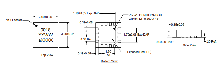
TQP3M9018 Dimensions
Notes:
- All measurements are in millimeters; angles are in degrees.
- Dimensions and tolerances follow the ASME Y14.4M-1994 standard.
- Terminal #1 identification and numbering follow JESD 95-1 SPP-012 standards.
TQP3M9018 Pad Configuration and Description
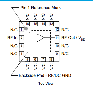
TQP3M9018 Functional Block Diagram
Recommended PCB Layout Pattern
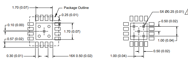
COMPONENT SIDE
Notes:
- All dimensions are in millimeters (inches); angles are in degrees.
- Use a minimum of 1 oz. copper for both top and bottom PCB layers.
- Ground and thermal vias are required for proper device operation. Recommended via drill: 0.35 mm (#80 / 0.0135”) with a finished plated thru diameter of 0.25 mm (0.010”).
- Ensure a solid solder connection for the package backside exposed pad (EP) to achieve optimal electrical and thermal performance.
Tape and Reel Information – Carrier and Cover Tape Dimensions
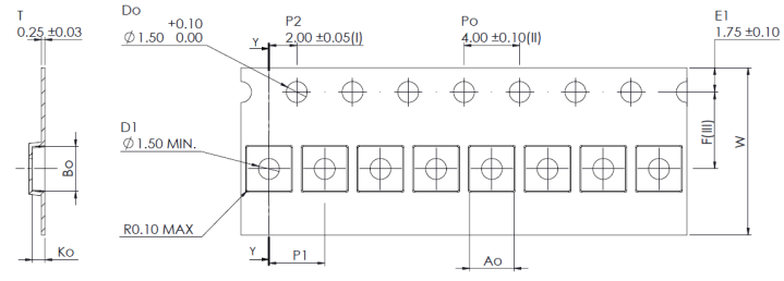
Feature Dimensions – Carrier Tape
| Feature | Measurement | Symbol | Size (in) | Size (mm) |
|---|---|---|---|---|
| Cavity Length | — | A0 | 0.125 | 3.20 |
| Cavity Width | — | B0 | 0.125 | 3.20 |
| Cavity Depth | — | K0 | 0.039 | 1.00 |
| Cavity Pitch | — | P1 | 0.157 | 4.00 |
| Centerline Distance – Cavity to Perforation (Length Direction) | — | P2 | 0.079 | 2.00 |
| Centerline Distance – Cavity to Perforation (Width Direction) | — | F | 0.217 | 5.50 |
| Carrier Tape Width | — | W | 0.472 | 12.0 |
Tape and Reel Information – Reel Dimensions
Standard T/R size = 2,500 pieces on a 7” reel.
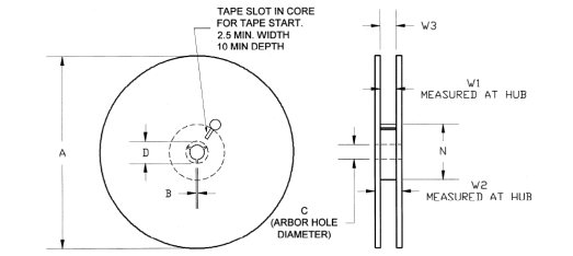
Tape and Reel Information – Reel Dimensions
Feature Dimensions – Reel / Flange
| Feature | Measurement | Symbol | Size (in) | Size (mm) |
|---|---|---|---|---|
| Flange Diameter | — | A | 6.969 | 177.00 |
| Flange Thickness | — | W2 | 0.717 | 18.20 |
| Space Between Flanges | — | W1 | 0.504 | 12.80 |
| Hub Outer Diameter | — | N | 2.283 | 58.00 |
| Arbor Hole Diameter | — | C | 0.512 | 13.00 |
| Key Slit Width | — | B | 0.079 | 2.00 |
| Key Slit Diameter | — | D | 0.787 | 20.00 |
Handling Precautions
| Parameter | Rating | Standard |
|---|---|---|
| ESD – Human Body Model (HBM) | 1A | ESDA / JEDEC JS-001-2017 |
| ESD – Charged Device Model (CDM) | C3 | JEDEC JESD22-C101F |
| MSL – Moisture Sensitivity Level | Level 1 | IPC/JEDEC J-STD-020E |
Caution: ESD-sensitive device. Proper handling procedures must be followed to avoid damage.
Solderability:
- Compatible with lead-free soldering (max 260 °C reflow) and tin/lead soldering (max 245 °C reflow).
- Soldering profiles available upon request.
- Contact plating: Annealed matte tin.
RoHS Compliance:
- Fully compliant with 2011/65/EU RoHS directive, as amended by 2015/863/EU.
- Additional attributes: Lead-free Halogen-free (no Chlorine or Bromine) Antimony-free TBBP-A (C15H12Br402) free PFOS free SVHC free
Pad Descriptions
| Pad No. | Label | Description |
|---|---|---|
| 2 | RF In | RF input, matched to 50 Ω. Requires an external DC block. |
| 11 | RF Out / VDD | RF output, matched to 50 Ω. Requires bias voltage and an external DC block. |
| All other pins | N/C | No internal connection. Provide grounded PCB pads for optimal isolation and secure mounting. |
| Backside Pad | RF/DC GND | RF/DC ground. Use the recommended via pattern to minimize inductance and thermal resistance. Refer to the PCB Mounting Pattern. |
Ordering Information
| Part Number | Description |
|---|---|
| TQP3M9018 | 2500 units on a 7-inch reel |
| TQP3M9018-PCB_IF | Evaluation board for 50–500 MHz range |
| TQP3M9018-PCB_RF | Evaluation board for 0.5–4 GHz range |
Absolute Maximum Ratings
| Parameter | Rating |
|---|---|
| Storage Temperature | −65 to +150 °C |
| RF Input Power (CW, 50 Ω, T=25 °C) | +23 dBm |
| Supply Voltage (VDD) | +7 V |
| Reverse Supply Voltage | −0.3 V |
Note: Exceeding one or more of these absolute maximum limits may result in permanent device damage.
Recommended Operating Conditions
| Parameter | Min | Typ | Max | Units |
|---|---|---|---|---|
| Supply Voltage (VDD) | +3.0 | +5.0 | +5.25 | V |
| Case Temperature (TCASE) | −40 | — | +105 | °C |
| Junction Temperature for >10⁶ hours MTTF (Tj) | — | — | +190 | °C |
Note: Electrical specifications are validated under defined test conditions. Performance is not guaranteed across all recommended operating conditions. Using the device outside these ranges may impact reliability and degrade performance.
Electrical Specifications
Test conditions (unless otherwise stated): VDD = +5 V, Temperature = +25 °C, 50 Ω system
| Parameter | Conditions | Min | Typ | Max | Units |
|---|---|---|---|---|---|
| Operational Frequency Range | — | 20 | — | 4000 | MHz |
| Test Frequency | — | — | 1900 | — | MHz |
| Gain | — | 19 | 20.5 | 22 | dB |
| Input Return Loss | — | — | 16 | — | dB |
| Output Return Loss | — | — | 19 | — | dB |
| Output P1dB | — | — | +21 | — | dBm |
| Output IP3 | Pout = +3 dBm/tone, Δf = 1 MHz | +33 | +37 | — | dBm |
| Noise Figure | — | — | 1.3 | — | dB |
| Current, IDD | — | 85 | — | 100 | mA |
| Thermal Resistance, θJC | Junction to case | — | 38.7 | — | °C/W |
Evaluation Board – TQP3M9018-PCB_RF (500-4000 MHz)
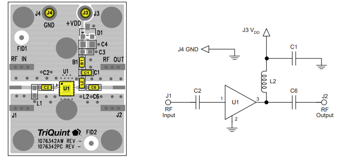
Evaluation Board – TQP3M9018-PCB_RF (500-4000 MHz)
Notes:
- Refer to the Evaluation Board PCB Information section for details on materials and stack-up.
- Components marked on the silkscreen but missing from the schematic are not populated.
- B1 (0 Ω jumper), though not shown in the schematic, may be substituted with a copper trace in the final application layout.
- Recommended component values vary depending on the operating frequency.
- Unless otherwise noted, all components are 0603 size.
Bill of Materials – TQP3M9018-PCB_RF (500–4000 MHz)
| Reference Designator | Value | Description | Manufacturer / Part Number |
|---|---|---|---|
| n/a | n/a | Printed Circuit Board | Qorvo 1076342 |
| U1 | n/a | High Linearity LNA Gain Block | Qorvo TQP3M9018 |
| C2, C6 | 100 pF | Capacitor, 0603, 5%, 100 V, NPO/COG | Various |
| C1 | 0.01 µF | Capacitor, 0603, 5%, 50 V, X7R | Various |
| L2 | 68 nH | Inductor, 0603, 5% | Coilcraft 0603CS-68NXJL |
| B1 | 0 Ω | Resistor, 0603 | Various |
| L1, D1, C3, C4 | DNP | Not populated | — |
Notes:
- Performance can be fine-tuned for the desired frequency using the recommended component values listed below.
- Inductors are wirewound Coilcraft types.
Recommended Component Values by Frequency
| Reference Designator | 50 MHz | 200 MHz | 500 MHz | 2000 MHz | 2500 MHz | 3500 MHz |
|---|---|---|---|---|---|---|
| C2, C6 | 0.01 µF | 1000 pF | 100 pF | 22 pF | 22 pF | 22 pF |
| L2 | 470 nH | 220 nH | 82 nH | 22 nH | 18 nH | 15 nH |
Typical Performance – TQP3M9018-PCB_RF
Test conditions unless otherwise noted: VDD = +5 V, IDD = 85 mA (typical), Temperature = +25 °C
| Parameter | 500 MHz | 900 MHz | 1900 MHz | 2700 MHz | 3500 MHz | 4000 MHz | Units |
|---|---|---|---|---|---|---|---|
| Gain | 22.4 | 21.9 | 20.5 | 19.5 | 18.2 | 17 | dB |
| Input Return Loss | 10 | 11 | 16.6 | 30.5 | 12.7 | 8 | dB |
| Output Return Loss | 9 | 10 | 19 | 16 | 16.6 | 18 | dB |
| Output P1dB | +21.4 | +21.4 | +21 | +20.2 | +19.8 | +19.2 | dBm |
| OIP3 (1) | +38.4 | +37.5 | +37 | +35.3 | +34.7 | +34.4 | dBm |
| Noise Figure (2) | 1.1 | 1.1 | 1.3 | 1.6 | 2 | 2.5 | dB |
Notes:
- OIP3 measured using two tones at +4 dBm per tone, separated by 1 MHz.
- Noise figure values include PCB losses (approximately 0.1 dB at 2 GHz).
Performance Plots – TQP3M9018-PCB_RF
Test conditions unless otherwise specified: VDD = +5 V, IDD = 85 mA (typical), Temperature = +25 °C
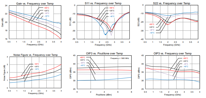
Performance Plots – TQP3M9018-PCB_RF
Performance Plots – TQP3M9018-PCB_RF
Test conditions unless otherwise noted: VDD=+5V, IDD=85 mA typ., Temp= +25°C
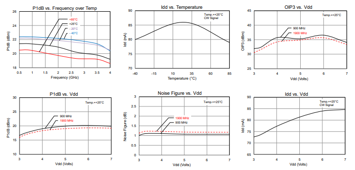
Performance Plots – TQP3M9018-PCB_RF
Conclusion
The TQP3M9018 is a high-linearity, low-noise gain block covering 20 MHz to 4 GHz, offering excellent gain, linearity, and low noise in a compact 16‑pin QFN package. Its wide frequency range, robust performance, and ease of integration make it ideal for wireless infrastructure, repeaters, and other high-performance transmitter and receiver applications.
Contact us today for a TQP3M9018 quote!
Looking for a high-performance LNA gain block? The TQP3M9018 delivers wideband coverage from 20 MHz to 4 GHz, high gain, low noise, and excellent linearity—all in a compact 16‑pin QFN package. Perfect for wireless infrastructure, repeaters, and advanced RF systems.
Contact us today for a quote! Our team at JMBom will provide you with the best pricing and fastest response to meet your project needs.

Amanda Miller
Amanda Miller is a senior electronics engineer with 6 years of experience. She focuses on studying resistors, transistors, and package design in detail. Her deep knowledge helps her bring innovation and high standards to the electronics industry.
Subscribe to JMBom Electronics !