


Qorvo QPA2610 GaN Power Amplifier Datasheet
Catalog
Product OverviewIntroduction to the QPA2610Key FeaturesApplicationsDesign ConsiderationsBenefits of Using the QPA2610Comparison with Traditional AmplifiersTechnical SpecificationsQPA2610 Functional Block DiagramTest Conditions (unless otherwise specified)ConclusionProduct Overview
Qorvo’s QPA2610 is a high-performance packaged power amplifier, built using Qorvo’s 0.15 µm GaN on SiC production process (QGaN15). Designed for operation across 8.5 – 10.5 GHz, the QPA2610 delivers more than 2 W of saturated output power with 23 dB large-signal gain, and achieves an impressive 47% power-added efficiency (PAE).
Housed in a compact 5 x 5 mm plastic overmold QFN package, it supports the tight spacing requirements of phased array radar systems. Both the RF input and output ports are 50 Ω matched and feature integrated DC blocking capacitors. The QPA2610 belongs to a three-amplifier family and is pin-compatible with the QPA2611 and QPA2612.
This product is lead-free and RoHS compliant.
Introduction to the QPA2610
The QPA2610 is a packaged GaN (Gallium Nitride) power amplifier that operates across wide frequency ranges. Gallium Nitride technology has transformed RF and microwave design because of its ability to handle high voltages and currents while maintaining efficiency. With GaN-based design, the QPA2610 can achieve high gain, robust output power, and better thermal management compared to traditional technologies such as GaAs or LDMOS.
Packaged amplifiers like the QPA2610 also bring the advantage of simplifying integration. Instead of designing a discrete amplifier from scratch, engineers can use the ready-to-implement module, which reduces development time and risk.
Key Features
- Frequency Range: 8.5 – 10.5 GHz
- Output Power (PIN = 10 dBm): > 33 dBm
- PAE (PIN = 10 dBm): > 47%
- Small-Signal Gain: > 37.5 dB
- Input Return Loss: > 14 dB
- Output Return Loss: > 12 dB
- Recommended Bias: VD = 20 V, IDQ = 56 mA
- Package Dimensions: 5.0 × 5.0 × 0.85 mm
Applications
- Radar Systems
- Wireless Communications
- Satellite Communications (Satcom)
The QPA2610 can be used across a variety of systems that require high output power and wideband operation. Key applications include:
- Radar SystemsRadar applications require high-power amplifiers to ensure that transmitted signals can travel long distances and return with enough strength for detection. The QPA2610’s high output power and broadband capabilities make it suitable for radar in both defense and weather monitoring systems.
- Electronic Warfare (EW)In defense electronics, electronic warfare systems rely on amplifiers capable of wideband operation and rapid power delivery. The QPA2610 fits well into such designs, providing reliable performance under harsh conditions.
- Satellite Communications (SATCOM)SATCOM systems need amplifiers that provide high linearity and efficiency to maintain clear and reliable communication links. The QPA2610 offers these capabilities, making it a good fit for ground stations and airborne platforms.
- Wireless InfrastructureBase stations and wireless infrastructure require linear, efficient amplifiers to handle high data throughput. The QPA2610 provides a high-power solution for emerging communication standards.
- Test and Measurement EquipmentHigh-performance test equipment often includes RF amplifiers to evaluate devices across wide frequency ranges. The QPA2610 ensures consistent and repeatable results for such systems.
Design Considerations
When designing with the QPA2610, engineers need to take into account several factors:
- Thermal ManagementHigh-power amplifiers generate substantial heat. Proper thermal design, including heat sinks and efficient PCB layout, ensures that the QPA2610 performs reliably over time.
- Impedance MatchingEven though the packaged amplifier simplifies matching, designers should still verify that the surrounding RF circuitry is optimized for 50-ohm systems to minimize losses and maximize performance.
- Power Supply RequirementsThe QPA2610 requires a suitable DC supply voltage, often higher than traditional technologies because of GaN’s capabilities. Engineers should design stable and clean power delivery.
- Linearity vs. Efficiency Trade-offsFor communication systems, linearity is critical, while radar and EW applications may prioritize raw output power. Designers should tune the amplifier’s operation according to the system’s primary requirement.
- Reliability in Harsh EnvironmentsApplications such as defense and satellite systems expose electronics to extreme conditions. The QPA2610’s GaN foundation makes it robust, but careful system-level design ensures maximum lifespan.
Benefits of Using the QPA2610
Using the QPA2610 brings multiple benefits:
- Faster Time-to-Market – With a packaged design, engineers can integrate the amplifier quickly without spending months on custom amplifier development.
- Improved System Performance – The amplifier’s combination of gain, output power, and efficiency boosts overall system capability.
- Versatility – With broadband performance, a single amplifier can serve multiple frequency bands, reducing the need for multiple components.
- Reduced System Complexity – High gain and integrated packaging reduce the number of additional amplifier stages and supporting circuitry.
- High Reliability – GaN technology and thermal design enable robust long-term operation.
Comparison with Traditional Amplifiers
Compared to traditional GaAs or LDMOS amplifiers, the QPA2610’s GaN foundation provides:
- Higher Power Density – More power in a smaller footprint.
- Better Efficiency – Reducing power consumption and heat generation.
- Broader Bandwidth – Supporting multiple applications with one device.
- Ruggedness – Withstanding high voltages and harsh conditions.
This makes GaN-based solutions like the QPA2610 the preferred choice for next-generation RF and microwave systems.
Technical Specifications
While exact values depend on the datasheet, some general specifications for the QPA2610 include:
- Frequency Range: Designed for broadband operation, often spanning multiple GHz.
- Output Power (Psat): High saturated output power suitable for radar, communications, and test equipment.
- Gain: Typically high gain to reduce the need for multiple amplifier stages.
- Efficiency: GaN devices usually achieve superior efficiency compared to traditional semiconductor technologies.
- Package Type: Packaged solution for straightforward PCB integration.
- Thermal Resistance: Optimized for high-reliability operation under elevated temperatures.
These specifications make the QPA2610 a competitive choice in high-power RF designs.
QPA2610 Functional Block Diagram
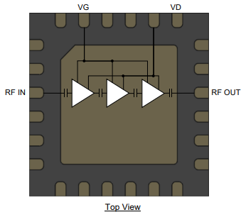
QPA2610 Functional Block Diagram
Absolute Maximum Ratings
| Parameter | Rating |
|---|---|
| Drain Voltage (VD) | 29.5 V |
| Gate Voltage Range (VG) | −4 to 0 V |
| Drain Current (ID) | 700 mA |
| Gate Current (IG) | See plot (pg. 16) |
| Power Dissipation (PDISS), TBASE = 85 °C | 8.8 W |
| Input Power (PIN), Pulsed (100 µs / 10%), 50 Ω, VD = 20 V, TBASE = 85 °C | 18 dBm |
| Input Power (PIN), Pulsed (100 µs / 10%), VSWR 3:1, VD = 20 V, TBASE = 85 °C | 18 dBm |
| Mounting Temperature (30 seconds max.) | 260 °C |
| Storage Temperature | −55 to +150 °C |
Important Note:
Exceeding one or more of the above absolute maximum ratings can cause irreversible damage to the device. Prolonged operation under these limits may also reduce long-term reliability.
Recommended Operating Conditions
| Parameter | Typical Value |
|---|---|
| Drain Voltage (VD) | 20 V |
| Quiescent Drain Current (IDQ) | 56 mA |
| Drain Current Under RF Drive (ID_DRIVE) | See plots (pg. 4) |
| Gate Voltage Range (VG) | −2.8 to −2.0 V |
| Gate Current Under RF Drive (IG_DRIVE) | See plots (pg. 4) |
Note:
Electrical performance values are measured under specific test conditions. They are not guaranteed across the full range of recommended operating conditions.
Electrical Specifications
| Parameter | Conditions | Min | Typ | Max | Units |
|---|---|---|---|---|---|
| Operational Frequency | — | 8.5 | — | 10.5 | GHz |
| Output Power (PIN = 10 dBm) | Pulsed, VD | — | 33.9 | — | dBm |
| Power Added Efficiency (PIN = 10 dBm) | Pulsed, VD | — | 47.4 | — | % |
| Small-Signal Gain | CW | — | 38.5 | — | dB |
| Input Return Loss | CW | — | 19 | — | dB |
| Output Return Loss | CW | — | 14 | — | dB |
| 3rd Order IMD (PIN/Tone = 0 dBm) | 10 MHz tone spacing | — | −15 | — | dBc |
| Output Power Temp. Coefficient | 85 °C → 25 °C, PIN = 10 dBm | — | −0.21 | — | dB/°C |
| Small-Signal Gain Temp. Coefficient | 85 °C → −40 °C | — | −0.09 | — | dB/°C |
| Gate Leakage Current | VD = 10 V, VG = −3.7 V | — | −1.23 | — | mA |
Test Conditions (unless otherwise specified)
T = +25 °C, VD = 20 V, IDQ = 56 mA, Pulse Width = 100 µs, Duty Cycle = 10%
Performance Plots – Large Signal (Pulsed)
Test conditions unless otherwise noted: T = +25 °C, VD = 20 V, IDQ = 56 mA, PIN = 10 dBm, Pulse Width = 100 us, Duty Cycle = 10%
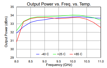
Output Power vs. Freq. vs. Temp.
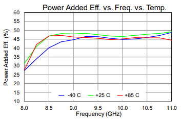
Power Added Eff. vs. Freq. vs. Temp
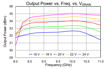
Output Power vs. Freq. vs. VDRAIN
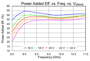
Power Added Eff. vs. Freq. vs. VDRAIN
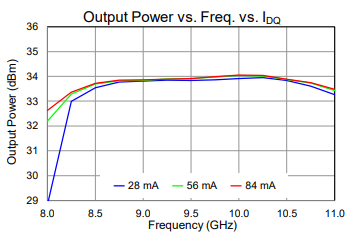
Output Power vs. Freq. vs. IDQ
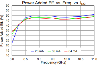
Power Added Eff. vs. Freq. vs. IDQ
Conclusion
The Qorvo QPA2610 is a high-performance packaged power amplifier that brings together the advantages of GaN technology, robust packaging, and broadband operation. With high output power, strong gain, and excellent efficiency, it meets the needs of applications ranging from radar and electronic warfare to satellite communications and wireless infrastructure. Its packaged format simplifies design and reduces time-to-market, while its reliability ensures long-term performance in even the harshest environments. For engineers seeking a powerful and versatile RF amplifier solution, the QPA2610 stands out as a top choice.

Christopher Anderson
Christopher Anderson has a Ph.D. in electrical engineering, focusing on power electronics. He’s been a Senior member of the IEEE Power Electronics Society since 2021. Right now, he works with the KPR Institute of Engineering and Technology in the U.S. He also writes detailed, top-notch articles about power electronics for business-to-business electronics platforms.
Subscribe to JMBom Electronics !


