


HMC565LC5 GaAs pHEMT MMIC Low Noise Amplifier – Overview and Specifications
Catalog
OverviewKey FeaturesTypical ApplicationsFunctional DiagramElectrical SpecificationsGaAs SMT PHEMT LOW NOISEOutline DrawingPin DescriptionsEvaluation PCBList of Materials for Evaluation PCB 110431ConclusionFAQ – HMC565LC5 GaAs pHEMT MMIC Low Noise AmplifierOverview
The HMC565LC5 is a GaAs pHEMT MMIC Low Noise Amplifier designed for high dynamic range applications. It comes in a compact, leadless, RoHS-compliant 5 × 5 mm surface-mount package. Operating across the 6–20 GHz range, this LNA delivers 21 dB small-signal gain, a low 2.5 dB noise figure, and an output IP3 of +20 dBm. With its self-biased design, single +3V power supply, and DC-blocked RF I/Os, the HMC565LC5 is well-suited for use in microwave radio systems.
HMC565LC5 GaAs pHEMT MMIC Low Noise Amplifier
Key Features
- Low Noise Figure: 2.5 dB
- High Gain: 21 dB
- Output IP3: +20 dBm
- Single Supply: +3V @ 53 mA
- 50 Ohm Matched Input/Output
- Compact RoHS-Compliant 5 × 5 mm SMT Package
Typical Applications
The HMC565LC5 is well-suited for use as a low-noise amplifier or driver amplifier in:
- Point-to-Point Radio Systems
- Point-to-Multi-Point Radios and VSAT Terminals
- Test and Measurement Equipment, as well as Sensors
- Military and Aerospace Applications
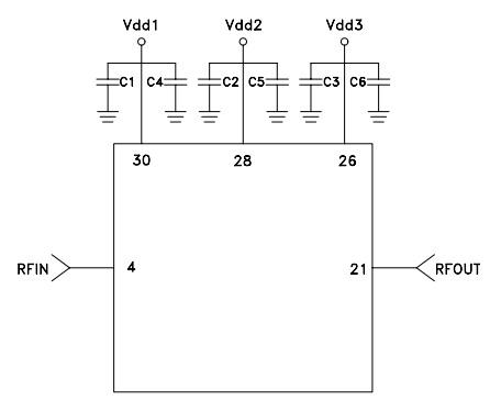
Functional Diagram
Electrical Specifications
(TA = +25 °C, Vdd1/2/3 = +3V)
| Parameter | Min | Typ | Max | Min | Typ | Max | Units |
|---|---|---|---|---|---|---|---|
| Frequency Range | 6 – | – | 12 | 12 – | – | 20 | GHz |
| Gain | 19 | 21 | – | 16 | 18.5 | – | dB |
| Gain Variation vs. Temperature | – | 0.025 | 0.035 | – | 0.025 | 0.035 | dB/°C |
| Noise Figure | – | 2.5 | 2.8 | – | 2.5 | 3.0 | dB |
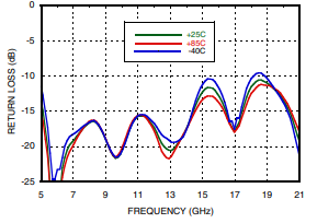
| Input Return Loss | – | 15 | – | – | 12 | – | dB |
| Output Return Loss | – | 13 | – | – | 15 | – | dB |
| Output Power @ 1 dB Compression (P1dB) | 8 | 10 | – | 9 | 11 | – | dBm |
| Saturated Output Power (Psat) | – | 11 | 13 | – | – | – | dBm |
| Third-Order Output Intercept (IP3) | – | 20 | 21 | – | – | – | dBm |
| Supply Current (Idd) @ +3V | – | 53 | 75 | – | 53 | 75 | mA |
GaAs SMT PHEMT LOW NOISE
AMPLIFIER, 6 - 20 GHz
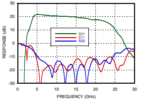
Broadband Gain & Return Loss
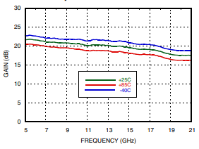
Gain vs. Temperature
Input Return Loss vs. Temperature
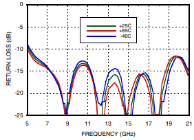
Output Return Loss vs. Temperature
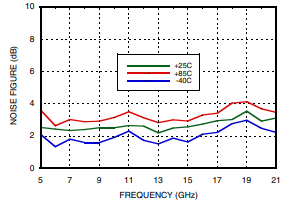
Noise Figure vs. Temperature
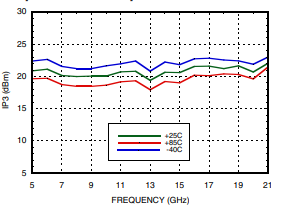
Output IP3 vs. Temperature
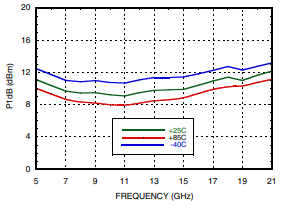
P1dB vs. Temperature
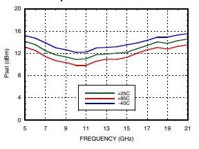
Psat vs. Temperature
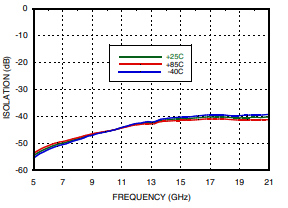
Reverse Isolation vs. Temperature
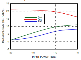
Power Compression @ 12 GHz
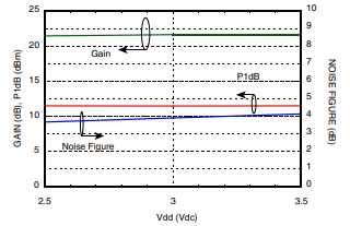
Gain, Noise Figure & Power vs.
Supply Voltage @ 12 GHz
Absolute Maximum Ratings
- Drain Bias Voltage (Vdd1, Vdd2, Vdd3): +3.5 Vdc
- RF Input Power (RFIN) @ Vdd = +3.0 Vdc: 10 dBm
- Channel Temperature: 175 °C
- Continuous Power Dissipation (Pdiss @ 85 °C): 0.753 W (Derate at 8.5 mW/°C above 85 °C)
- Thermal Resistance (Channel to Ground Paddle): 119.5 °C/W
- Storage Temperature Range: –65 °C to +150 °C
- Operating Temperature Range: –40 °C to +85 °C
- ESD Sensitivity (HBM): Class 1A
Outline Drawing
![32-Terminal Ceramic Leadless Chip Carrier [LCC] (E-32-1) Dimensions shown in millimeters](https://res.jmbom.com/upload/2025/9/1759039556919844.webp)
32-Terminal Ceramic Leadless Chip Carrier [LCC]
(E-32-1)
Dimensions shown in millimeters
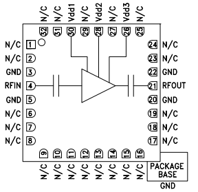
Pin Descriptions
| Pin Number | Function | Description |
|---|---|---|
| 1, 2, 6–19, 23–25, 27, 29, 31, 32 | N/C | No connection. These pins may be tied to RF/DC ground without affecting performance. |
| 3, 5, 20, 22 | GND | Ground. These pins, along with the exposed package paddle, must be connected to RF/DC ground. |
| 4 | RFIN | RF input. This pin is AC-coupled and internally matched to 50 Ω. |
| 21 | RFOUT | RF output. This pin is AC-coupled and internally matched to 50 Ω. |
| 30, 28, 26 | Vdd1, Vdd2, Vdd3 | Power supply inputs for the amplifier. External bypass capacitors of 100 pF and 2.2 µF are required. |
Application Circuit
Component Values
- C1, C2, C3: 100 pF
- C4, C5, C6: 2.2 µF
Application Circuit
Evaluation PCB
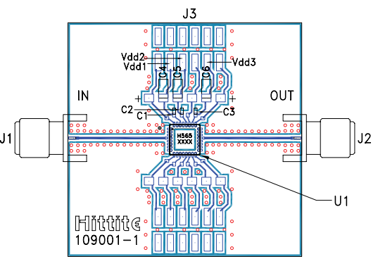
Evaluation PCB
List of Materials for Evaluation PCB 110431
The application circuit board should follow standard RF design practices. Signal traces must be designed for 50 Ω impedance, and the package ground pins along with the exposed paddle should be tied directly to the ground plane as illustrated. A sufficient number of vias must be included to ensure solid connection between the top and bottom ground planes. For proper thermal management, the evaluation board should be mounted to a suitable heat sink.
The evaluation PCB shown is available from Analog Devices upon request.
Bill of Materials
- J1 – J2: PCB-Mount K Connectors
- J3: 2 mm DC Header
- C1 – C3: 100 pF Capacitors, 0402 Package
- C4 – C6: 2.2 µF Tantalum Capacitors
- U1: HMC565LC5 Amplifier
- PCB [2]: 109001 Evaluation Board
Notes:
[1] Use this reference number when ordering the complete evaluation PCB.
[2] PCB material: Rogers 4350.
Conclusion
The HMC565LC5 GaAs pHEMT MMIC Low Noise Amplifier combines wideband performance, low noise, and high linearity in a compact 5 × 5 mm SMT package. With simple +3V single-supply operation, excellent RF characteristics, and proven reliability, it is well-suited for demanding applications in communications, test equipment, military, and aerospace systems. Its balance of ease of integration and robust performance makes it a versatile choice for modern RF designs.
FAQ – HMC565LC5 GaAs pHEMT MMIC Low Noise Amplifier
What is the HMC565LC5 and what makes it unique?
The HMC565LC5 is a gallium arsenide (GaAs) pseudomorphic high electron mobility transistor (pHEMT) monolithic microwave integrated circuit (MMIC) low noise amplifier (LNA). What makes it stand out is its combination of wide frequency coverage (6 to 20 GHz), excellent noise performance (as low as 2.5 dB), and strong linearity with an output IP3 of +20 dBm. Unlike many other amplifiers in this frequency range, the HMC565LC5 is self-biased, meaning it requires minimal external circuitry to operate. Packaged in a compact 5 × 5 mm RoHS-compliant SMT housing, it offers designers a reliable and space-efficient solution for microwave radio, radar, and satellite communication systems.
What are the main performance specifications of the HMC565LC5?
Key specifications include a gain of 19–21 dB in the 6–12 GHz range and 16–18.5 dB in the 12–20 GHz range. The noise figure is typically 2.5–2.8 dB, which is excellent for high-frequency low-noise designs. Its output third-order intercept point (IP3) is typically +20 to +21 dBm, while the output power at 1 dB compression (P1dB) is 8–11 dBm depending on the frequency band. The amplifier runs from a single +3V supply, drawing around 53 mA of current under normal operation. These specifications make it ideal for applications where both sensitivity and linearity are critical.
What applications are best suited for the HMC565LC5?
The HMC565LC5 is highly versatile and can be deployed in a variety of RF and microwave systems. Common applications include point-to-point and point-to-multipoint radio links, VSAT terminals for satellite communications, test and measurement equipment requiring high-frequency low-noise amplification, and radar or sensor systems where low distortion and high gain are essential. It is also used in military and aerospace applications thanks to its wide operating temperature range (–40 °C to +85 °C) and high channel temperature tolerance (up to 175 °C).
How does the noise performance of the HMC565LC5 benefit RF system design?
The noise figure of an amplifier determines how much additional noise is introduced into the signal chain. With a noise figure as low as 2.5 dB, the HMC565LC5 ensures that the system maintains high sensitivity, which is especially important in weak signal environments such as long-distance satellite links or deep-space communication. By keeping the system noise contribution low, designers can achieve better signal-to-noise ratios (SNR), leading to improved receiver performance and overall system reliability.
What power supply requirements does the HMC565LC5 have?
The amplifier operates from a single +3V supply, making it easy to integrate into modern RF systems without requiring multiple supply voltages. It typically draws 53 mA of current, with a maximum of 75 mA under specified conditions. For stable operation, external bypass capacitors are required on the supply lines: usually a combination of 100 pF (for high-frequency decoupling) and 2.2 µF (for low-frequency filtering). This ensures the amplifier remains stable and free from unwanted oscillations caused by supply noise.
How should the HMC565LC5 be integrated into a PCB design?
When integrating the HMC565LC5 into a circuit board, standard RF design practices must be followed. Signal traces should be designed for 50-ohm impedance, and both the package ground pins and the exposed ground paddle must be soldered directly to the ground plane. A generous number of vias should connect the top and bottom ground planes to minimize inductance and ensure solid grounding. The amplifier should also be mounted with adequate thermal management, such as on a heat-sinked PCB, to maintain performance and reliability at higher power levels.
What are the absolute maximum ratings and why are they important?
The absolute maximum ratings define the limits beyond which permanent damage may occur. For the HMC565LC5, the drain bias voltage should not exceed +3.5 V, RF input power should be limited to +10 dBm when Vdd is +3V, and the channel temperature must not surpass 175 °C. Storage temperature is between –65 °C and +150 °C, while the safe operating range is –40 °C to +85 °C. Exceeding these limits can lead to device degradation, reliability issues, or complete failure. Designers should always ensure that the amplifier is operated within recommended conditions to achieve long service life.
What packaging and mounting options are available?
The HMC565LC5 comes in a compact 5 × 5 mm leadless surface-mount package that is RoHS compliant. The package includes multiple ground pins and a large exposed paddle for both electrical and thermal grounding. This design minimizes parasitics at high frequencies and helps maintain consistent performance across its 6–20 GHz range. Being SMT-compatible, it is suitable for automated PCB assembly processes, which is important for high-volume manufacturing.
What evaluation boards or reference designs are available?
Analog Devices offers an evaluation PCB (part number 109001) for testing and characterizing the HMC565LC5. The board is designed using Rogers 4350 material, which has excellent RF performance characteristics. It includes all necessary bypass capacitors, RF connectors, and headers to allow easy connection to lab test equipment. By using the evaluation board, engineers can quickly measure gain, noise figure, linearity, and other parameters under real-world conditions without needing to design a custom test fixture.
How does the HMC565LC5 compare to other LNAs in its class?
Compared to other LNAs covering the 6–20 GHz range, the HMC565LC5 strikes an excellent balance between gain, noise performance, and linearity. While some LNAs may achieve slightly lower noise figures, they often come at the cost of reduced gain or linearity. Conversely, amplifiers with higher linearity often consume more power or require more complex biasing. The HMC565LC5, with its self-bias design and +3V single-supply operation, offers a simplified yet powerful solution, making it an attractive choice for engineers seeking both high performance and ease of integration.

Christopher Anderson
Christopher Anderson has a Ph.D. in electrical engineering, focusing on power electronics. He’s been a Senior member of the IEEE Power Electronics Society since 2021. Right now, he works with the KPR Institute of Engineering and Technology in the U.S. He also writes detailed, top-notch articles about power electronics for business-to-business electronics platforms.
Subscribe to JMBom Electronics !


