


OPx13 Key Features and Applications
Catalog
GENERAL DESCRIPTIONFEATURESAPPLICATIONSPIN CONFIGURATIONSSPECIFICATIONSSPECIFICATIONSAPPLICATIONSConclusionGENERAL DESCRIPTION
The OPx13 series of single-supply operational amplifiers combines low noise with minimal drift. They are specifically designed for systems that rely on internal calibration. While processor-based systems can often correct offset and gain errors, they generally cannot compensate for noise or temperature-related drift. The OPx13 series addresses these limitations, offering enhanced analog performance that works hand in hand with digital correction.
OPx13
Many internally calibrated systems run from unipolar supplies, typically 5 V or 12 V. The OPx13 series supports single-supply operation from 4 V to 36 V, while maintaining low-noise, high-precision performance.
This amplifier family is unity-gain stable and provides a typical gain-bandwidth product of 3.4 MHz, with a slew rate exceeding 1 V/μs. Noise density is just 4.7 nV/√Hz, and the 0.1 Hz to 10 Hz noise is 120 nV p-p. Input offset voltage is guaranteed, with an offset drift of less than 0.8 μV/°C. The input common-mode range spans the negative supply and extends to within 1 V of the positive supply across the full voltage range.
Built-in phase reversal protection prevents malfunction when the input exceeds its voltage range. Output swing covers the negative rail and reaches to within 1 V of the positive rail. The output stage can both source and sink current across its range, specified with loads as low as 600 Ω.
Digital scales and other strain gauge systems take advantage of the OPx13 family’s extremely low noise and minimal drift. They are also well-suited as buffers or amplifiers for sigma-delta ADCs and DACs, where low noise is essential to fully realize the high resolution of these converters.
Since many of these converters work in single-supply or low-voltage environments, maximizing signal swing is important for boosting overall system performance.
The OPx13 series is rated for operation with a single 5 V supply or dual ±15 V supplies, across the extended industrial temperature range (–40°C to +85°C). Devices are offered in both PDIP and SOIC surface-mount packages.
FEATURES
- Supports both single- and dual-supply operation
- Ultra-low noise: 4.7 nV/√Hz at 1 kHz
- Wide bandwidth: 3.4 MHz
- Low input offset voltage: 100 μV
- Excellent drift performance: 0.2 μV/°C
- Stable at unity gain
- Immune to phase reversal
APPLICATIONS
- Digital weighing scales
- Multimedia equipment
- Strain gauge systems
- Portable, battery-powered instruments
- Temperature sensor amplification
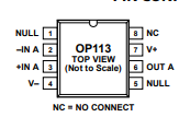
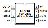
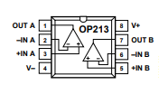
PIN CONFIGURATIONS
Lead Narrow-Body
SOIC_N
8-Lead Narrow-Body
SOIC_N
8-Lead PDIP
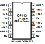
16-Lead Wide-Body
SOIC_W
SPECIFICATIONS
ELECTRICAL CHARACTERISTICS
(VS = ±15.0 V, TA = 25°C, unless otherwise specified)
| Parameter | Symbol | Conditions | E Grade Min | Typ | Max | F Grade Min | Typ | Max | Unit |
|---|---|---|---|---|---|---|---|---|---|
| INPUT CHARACTERISTICS | |||||||||
| Input Offset Voltage | VOS | OP113 | 75 | — | 150 | — | — | — | μV |
| −40°C ≤ TA ≤ +85°C | 125 | — | 225 | — | — | — | μV | ||
| OP213 | 100 | — | 250 | — | — | — | μV | ||
| −40°C ≤ TA ≤ +85°C | 150 | — | 325 | — | — | — | μV | ||
| OP413 | 125 | — | 275 | — | — | — | μV | ||
| −40°C ≤ TA ≤ +85°C | 175 | — | 350 | — | — | — | μV | ||
| Input Bias Current | IB | VCM = 0 V | — | 240 | 600 | — | — | 600 | nA |
| −40°C ≤ TA ≤ +85°C | — | — | 700 | — | — | 700 | nA | ||
| Input Offset Current | IOS | VCM = 0 V | — | — | — | — | — | 50 | nA |
| −40°C ≤ TA ≤ +85°C | — | — | — | — | — | 50 | nA | ||
| Input Voltage Range | VCM | — | −15 | — | +14 | −15 | — | +14 | V |
| Common-Mode Rejection | CMR | −15 V ≤ VCM ≤ +14 V | 100 | 116 | — | 96 | — | — | dB |
| −40°C ≤ TA ≤ +85°C | 97 | 116 | — | 94 | — | — | dB | ||
| Large-Signal Voltage Gain | AVO | OP113, OP213, RL = 600 Ω | 1 | — | 2.4 | 1 | — | — | V/μV |
| OP413, RL = 1 kΩ | 1 | — | 2.4 | 1 | — | — | V/μV | ||
| RL = 2 kΩ | 2 | — | 8 | 2 | — | — | V/μV | ||
| Long-Term Offset Voltage | VOS | — | — | 150 | 300 | — | — | — | μV |
| Offset Voltage Drift | ΔVOS/ΔT | — | — | 0.2 | 0.8 | — | — | 1.5 | μV/°C |
OUTPUT CHARACTERISTICS
| Parameter | Symbol | Conditions | Min | Typ | Max | Unit |
|---|---|---|---|---|---|---|
| Output Swing High | VOH | RL = 2 kΩ | 14 | — | — | V |
| −40°C ≤ TA ≤ +85°C | 13.9 | — | — | V | ||
| Output Swing Low | VOL | RL = 2 kΩ | −14.5 | — | — | V |
| −40°C ≤ TA ≤ +85°C | −14.5 | — | — | V | ||
| Short-Circuit Current | ISC | — | ±40 | — | — | mA |
POWER SUPPLY
| Parameter | Symbol | Conditions | Min | Typ | Max | Unit |
|---|---|---|---|---|---|---|
| Power Supply Rejection | PSRR | VS = ±2 V to ±18 V | 103 | 120 | — | dB |
| −40°C ≤ TA ≤ +85°C | 100 | 120 | — | dB | ||
| Supply Current per Amp | ISY | VOUT = 0 V, RL = ∞, VS = ±18 V | — | 3 | — | mA |
| −40°C ≤ TA ≤ +85°C | — | 3.8 | — | mA | ||
| Supply Voltage Range | VS | — | 4 | — | ±18 | V |
SPECIFICATIONS
AUDIO PERFORMANCE & DYNAMIC PERFORMANCE
(VS = 5.0 V, TA = 25°C, unless otherwise specified)
| Parameter | Symbol | Conditions | E Grade Min | Typ | Max | F Grade Min | Typ | Max | Unit |
|---|---|---|---|---|---|---|---|---|---|
| AUDIO PERFORMANCE | |||||||||
| Total Harmonic Distortion + Noise | THD+N | VIN = 3 Vrms, RL = 2 kΩ, f = 1 kHz | — | 0.0009 | — | — | 0.0009 | — | % |
| Voltage Noise Density | en | f = 10 Hz | — | 9 | — | — | 9 | — | nV/√Hz |
| f = 1 kHz | — | 4.7 | — | — | 4.7 | — | nV/√Hz | ||
| Current Noise Density | in | f = 1 kHz | — | 0.4 | — | — | 0.4 | — | pA/√Hz |
| Voltage Noise (peak-to-peak) | en p-p | 0.1 Hz to 10 Hz | — | 120 | — | — | 120 | — | nV p-p |
DYNAMIC PERFORMANCE | | | | | | | | | |
Slew Rate | SR | RL = 2 kΩ | 0.8 | 1.2 | — | 0.8 | 1.2 | — | V/μs |
Gain Bandwidth Product | GBP | — | — | 3.4 | — | — | 3.4 | — | MHz |
Channel Separation | — | VOUT = 10 V p-p, RL = 2 kΩ, f = 1 kHz | — | 105 | — | — | 105 | — | dB |
Settling Time | tS | To 0.01%, 0 V → 10 V step | — | 9 | — | — | 9 | — | μs |
Notes
- Long-term offset voltage is guaranteed through a 1000-hour life test on three independent lots at 125°C, with an LTPD of 1.3.
- Specifications are guaranteed based on characterization data.
SPECIFICATIONS
INPUT CHARACTERISTICS
| Parameter | Symbol | Conditions | Min | Typ | Max | Min | Typ | Max | Unit |
|---|---|---|---|---|---|---|---|---|---|
| Offset Voltage | VOS | OP113 | 125 | — | 175 | — | — | — | μV |
| −40°C ≤ TA ≤ +85°C | 175 | — | 250 | — | — | — | μV | ||
| OP213 | 150 | — | 300 | — | — | — | μV | ||
| −40°C ≤ TA ≤ +85°C | 225 | — | 375 | — | — | — | μV | ||
| OP413 | 175 | — | 325 | — | — | — | μV | ||
| −40°C ≤ TA ≤ +85°C | 250 | — | 400 | — | — | — | μV | ||
| Input Bias Current | IB | VCM = 0 V, VOUT = 2 | 300 | — | 650 | — | — | 650 | nA |
| −40°C ≤ TA ≤ +85°C | — | — | 750 | — | — | 750 | nA | ||
| Input Offset Current | IOS | VCM = 0 V, VOUT = 2 | — | — | — | — | — | 50 | nA |
| −40°C ≤ TA ≤ +85°C | — | — | — | — | — | 50 | nA | ||
| Input Voltage Range | VCM | — | 0 | — | 4 | 0 | — | 4 | V |
| Common-Mode Rejection | CMR | 0 V ≤ VCM ≤ 4 V | 93 | 106 | — | 90 | — | — | dB |
| −40°C ≤ TA ≤ +85°C | 90 | — | — | 87 | — | — | dB | ||
| Large-Signal Voltage Gain | AVO | OP113, OP213, RL = 600 Ω / 2 kΩ, 0.01 V ≤ VOUT ≤ 3.9 V | 2 | — | — | 2 | — | — | V/μV |
| OP413, RL = 600 Ω / 2 kΩ, 0.01 V ≤ VOUT ≤ 3.9 V | 1 | — | — | 1 | — | — | V/μV | ||
| Long-Term Offset Voltage¹ | VOS | — | 200 | — | 350 | — | — | — | μV |
| Offset Voltage Drift² | ΔVOS/ΔT | — | 0.2 | 1.0 | 1.5 | — | — | — | μV/°C |
Notes
- Long-term offset voltage is guaranteed by a 1000-hour life test performed on three independent lots at 125°C with an LTPD of 1.3.
- Specifications are guaranteed based on characterization data.
SPECIFICATIONS
(VS = as specified, TA = 25°C unless otherwise noted)
| Parameter | Symbol | Conditions | Min | Typ | Max | Min | Typ | Max | Unit |
|---|---|---|---|---|---|---|---|---|---|
| OUTPUT CHARACTERISTICS | |||||||||
| Output Voltage Swing High | VOH | RL = 600 kΩ | 4.0 | — | 4.0 | — | — | — | V |
| RL = 100 kΩ, −40°C ≤ TA ≤ +85°C | 4.1 | — | 4.1 | — | — | — | V | ||
| RL = 600 Ω, −40°C ≤ TA ≤ +85°C | 3.9 | — | 3.9 | — | — | — | V | ||
| Output Voltage Swing Low | VOL | RL = 600 Ω, −40°C ≤ TA ≤ +85°C | — | 8 | — | — | 8 | — | mV |
| RL = 100 kΩ, −40°C ≤ TA ≤ +85°C | — | 8 | — | — | 8 | — | mV | ||
| Short-Circuit Current | ISC | — | ±30 | — | ±30 | — | — | — | mA |
POWER SUPPLY | | | | | | | | | |
Supply Current | ISY | VOUT = 2.0 V, no load | 1.6 | — | 2.7 | — | — | 2.7 | mA |
| | −40°C ≤ TA ≤ +85°C | — | — | 3.0 | — | — | 3.0 | mA |
AUDIO PERFORMANCE | | | | | | | | | |
Total Harmonic Distortion + Noise | THD+N | VOUT = 0 dBu, f = 1 kHz | — | 0.001 | — | — | 0.001 | — | % |
Voltage Noise Density | en | f = 10 Hz | — | 9 | — | — | 9 | — | nV/√Hz |
| | f = 1 kHz | — | 4.7 | — | — | 4.7 | — | nV/√Hz |
Current Noise Density | in | f = 1 kHz | — | 0.45 | — | — | 0.45 | — | pA/√Hz |
Voltage Noise (p-p) | en p-p | 0.1 Hz to 10 Hz | — | 120 | — | — | 120 | — | nV p-p |
DYNAMIC PERFORMANCE | | | | | | | | | |
Slew Rate | SR | RL = 2 kΩ | 0.6 | 0.9 | — | 0.6 | — | — | V/μs |
Gain Bandwidth Product | GBP | — | — | 3.5 | — | — | 3.5 | — | MHz |
Settling Time | tS | To 0.01%, 2 V step | — | 5.8 | — | — | 5.8 | — | μs |
Notes
- Long-term offset voltage is guaranteed by a 1000-hour life test performed on three independent lots at 125°C with an LTPD of 1.3.
- All guaranteed specifications are based on characterization data.
ABSOLUTE MAXIMUM RATINGS
| Parameter | Rating |
|---|---|
| Supply Voltage | ±18 V |
| Input Voltage | ±18 V |
| Differential Input Voltage | ±10 V |
| Output Short-Circuit Duration to GND | Continuous |
| Storage Temperature Range | −65°C to +150°C |
| Operating Temperature Range | −40°C to +85°C |
| Junction Temperature Range | −65°C to +150°C |
| Lead Temperature (Soldering, 60 sec) | 300°C |
Note
Exceeding these ratings may cause permanent damage to the device. The values listed are stress ratings only. Operation at or beyond these conditions is not guaranteed and may impair functionality. Prolonged exposure to absolute maximum conditions can affect long-term reliability.
THERMAL RESISTANCE
| Package Type | θJA (°C/W) | θJC (°C/W) | Unit |
|---|---|---|---|
| 8-Lead PDIP (P) | 103 | 43 | °C/W |
| 8-Lead SOIC_N (S) | 158 | 43 | °C/W |
| 16-Lead SOIC_W (S) | 92 | 27 | °C/W |
Note
Thermal resistance values are measured under standard JEDEC test conditions. Actual performance may vary depending on PCB layout, airflow, and ambient conditions.
APPLICATIONS
The OP113, OP213, and OP413 belong to a high-performance amplifier family designed for precision operation in both standard dual-supply systems and single-supply configurations. Notably, they maintain accuracy even with single-supply operation. In addition to excellent dc characteristics, these devices deliver industry-leading low noise performance, with a typical noise density of only 4.7 nV/√Hz.
Single-supply designs often face challenges due to reduced dynamic range compared to dual-supply systems. Typical single-supply voltages of 5 V or 12 V limit the available output swing, whereas dual-supply systems (±12 V or ±15 V) can provide up to 20 V of output swing. To maximize usable range, single-supply output stages must be capable of swinging closer to the supply rails.
The OPx13 family employs a patented output stage that achieves output swings much closer to ground (or the negative rail) than traditional bipolar designs. Previous amplifiers could typically swing only within ~10 mV of the negative rail, while the OPx13 family—using a combined bipolar and CMOS output stage—can swing within just a few hundred microvolts of ground.
When operating at lower supply voltages, the input signal range is also constrained, reducing the achievable signal-to-noise ratio (SNR). Improving this requires either increasing signal swing or lowering noise. The OPx13 family achieves both:
- Wide Input Range: Extends from the negative rail to within 1 V of the positive rail across the full supply range. Competing devices typically offer 0.5 V to 5 V less range.
- Ultra-Low Noise: With 4.7 nV/√Hz, noise is less than one-quarter that of comparable amplifiers.
PHASE REVERSAL
The OPx13 family includes built-in protection against phase reversal as long as both inputs remain within the supply voltage range. If there is a risk that either input could fall below the negative supply (or ground in single-supply applications), it is recommended to add a series resistor to limit input current to 2 mA.
OP113 OFFSET ADJUST
The OP113 provides a standard external offset adjustment feature. Pins 1 and 5 are used with a 10 kΩ potentiometer, with the wiper connected to V− (or ground in single-supply systems). This setup allows an adjustment range of approximately ±2 mV.
Setting the offset to zero has minimal impact on offset drift, assuming the potentiometer has a temperature coefficient below 1000 ppm/°C. However, any adjustment away from zero will increase TCVOS (temperature coefficient of offset voltage) by about 3.3 μV/°C for every millivolt of induced offset, as is typical for bipolar amplifiers.
For this reason, using the trim to correct system-level errors outside the OP113 is generally not recommended. The OP113’s initial offset is low enough that external trimming is rarely necessary. If needed, the adjustment range can be reduced by using a 2 kΩ potentiometer, yielding a more practical ±400 μV range.
Conclusion
The OPx13 family of amplifiers offers high-precision performance, ultra-low noise, and flexibility for both single- and dual-supply applications. Built-in features like phase reversal protection and, in the case of the OP113, optional external offset adjustment provide reliability and fine-tuning capabilities. Careful consideration of input protection and offset trimming ensures optimal performance, making the OPx13 series suitable for precision analog applications where low noise, wide input range, and stable operation are critical.

Christopher Anderson
Christopher Anderson has a Ph.D. in electrical engineering, focusing on power electronics. He’s been a Senior member of the IEEE Power Electronics Society since 2021. Right now, he works with the KPR Institute of Engineering and Technology in the U.S. He also writes detailed, top-notch articles about power electronics for business-to-business electronics platforms.
Subscribe to JMBom Electronics !


