


AD8561 Hysteresis Configuration for Stable Switching
Catalog
OverviewKey FeaturesTypical ApplicationsAD8561 PIN CONFIGURATIONSApplicationsHysteresis ConfigurationConclusionOverview
The AD8561 is a high-speed 7 ns comparator featuring independent input and output sections. With separate power supplies, the input stage can operate from either ±5 V dual supplies or a +5 V single supply. Its fast 7 ns propagation delay makes it well-suited for timing circuits and line receiver applications. Rising and falling edge delays are closely matched and remain stable across temperature changes, ensuring accurate duty cycle transfer—an advantage for clock recovery systems.
AD8561
Designed with the same pin configuration as the LT1016, the AD8561 offers lower power consumption and a wider common-mode input range that extends to the negative supply rail. It is specified for industrial temperature conditions (–40°C to +85°C) and is available in 8-lead plastic DIP, 8-lead TSSOP, and 8-lead narrow SOIC surface-mount packages.
Key Features
- 7 ns propagation delay at 5 V
- Operates from a single 3 V to 10 V supply
- Low power consumption
- Built-in latch function
- Available in compact TSSOP packaging
Typical Applications
- High-speed timing circuits
- Clock recovery and distribution
- Line receiver systems
- Digital communication equipment
- Phase detection
- High-speed sampling
- Read channel detection
- PCMCIA card designs
- Drop-in replacement for LT1016
AD8561 PIN CONFIGURATIONS
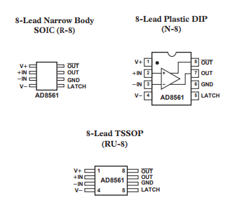
AD8561 PIN CONFIGURATIONS
Applications
Optimizing High-Speed Performance
As with any high-speed comparator or amplifier, proper circuit design and PCB layout are critical to getting the best results from the AD8561. The limits of high-speed circuits are often determined by stray capacitance, poor grounding, or layout issues.
To maximize performance, it’s important to minimize resistance between the signal source and the comparator input. Excessive source resistance, combined with input capacitance, can slow down response time. For example, 3 kΩ of source resistance with 5 pF of input capacitance produces a 15 ns time constant—slower than the AD8561’s 5 ns capability. For optimal performance, source resistance should be kept below 1 kΩ.
Power supply bypassing is also essential in high-speed applications. Place a 1 μF electrolytic capacitor within 0.5 inches of each power supply pin (Pin 1 and Pin 4) to ground. This helps filter out supply noise. Additionally, a 10 nF ceramic capacitor should be placed as close as possible to the power pins, providing a local charge reservoir during fast switching.
Using a ground plane is strongly recommended. A continuous conductive layer across the PCB, interrupted only where necessary for current paths, ensures a low-inductance ground. This reduces “ground bounce” and minimizes stray capacitance, both of which improve high-speed performance.
Replacing the LT1016
The AD8561 is pin-compatible with the LT1016 comparator, making it a straightforward upgrade. However, there are several important differences that should be considered to ensure proper operation. These include input voltage range, input bias currents, switching speed, output swing, and power consumption.
For example, when operating from a +5 V single supply, the LT1016 supports an input range of +1.25 V to +3.5 V, while the AD8561 offers a wider 0 V to 3.0 V range. Signals above 3.0 V can cause slower response times. If both input signals exceed 3.0 V, they should be shifted or attenuated to fit within the valid range. However, if only one signal slightly exceeds 3.0 V while the other remains well within the 0 V to 3.0 V range, the comparator may still operate reliably without circuit changes.
Comparator Example
Consider a case where the comparator compares a fast-changing input signal against a fixed 2.5 V reference. Since switching is only needed when the input is near 2.5 V, both signals remain within the valid input range (below 3.0 V) at the moment the comparator changes state.
However, if input voltages rise significantly above 3.0 V, input currents will increase and may slow down device response. The AD8561 has lower input bias current (–3 μA typical) compared to the LT1016 (+5 μA typical). The AD8561’s current flows out of the input pins, while the LT1016’s flows in. With low-value resistors or low-impedance signal sources, the resulting voltage shift from bias current will generally be negligible.
The AD8561 also operates faster (6.75 ns typical) than the LT1016 (10 ns typical). While this improved speed benefits many systems, timing adjustments may be required to take full advantage of the faster response. In addition, the AD8561 offers a wider output swing—extending from 0.2 V above ground to within 1.1 V of the positive supply—while consuming less power (5 mA typical) than the LT1016 (25 mA typical).
Increasing Output Swing
Although not essential for normal operation, output swing can be enhanced by connecting a 5 kΩ resistor from the output to V+. This method is especially useful in low-voltage supply applications where maximizing output range is important. Adding this pull-up resistor will not negatively affect the AD8561’s specifications.
Output Loading Considerations
The AD8561 output can source or sink up to 40 mA without noticeably affecting propagation delay. However, it should not be connected to more than 20 standard TTL input gates or loads below 100 Ω.
To maintain optimum performance, output capacitance should be minimized. Capacitive loads greater than 50 pF can cause output ringing and reduce the comparator’s effective bandwidth.
Latch Setup and Hold Times
The latch input (Pin 5) allows the AD8561 to hold its output state. When this pin is driven high, the output remains fixed regardless of the input signal.
- Setup time: 2–3 ns
- Hold time: 3 ns
This means the input must be valid at least 5 ns before the latch input goes high and remain valid for at least 3 ns after. Once the latch returns low, new data appears at the output within about 8 ns.
The latch recognizes logic high at ≥ +2.0 V and logic low at ≤ +0.8 V, ensuring straightforward compatibility with both TTL and CMOS logic. The latch circuitry itself has no built-in hysteresis.
Input Stage and Bias Currents
The AD8561 incorporates a PNP differential input stage, allowing the input common-mode voltage to range from the negative supply rail up to within 2.2 V of the positive rail. The common-mode voltage is defined as the average of the two input voltages. For best response time, inputs should remain within this range and not exceed the specified limits.
The typical input bias current of the AD8561 is 3 μA. In a PNP differential pair, this bias current goes to zero at the higher input and doubles at the lower input. Therefore, resistor values connected to the inputs should be carefully selected, since large resistance values can create noticeable voltage drops due to bias current.
The device has an input capacitance of approximately 3 pF. This value is determined by applying a 5 kΩ source resistance to the input and measuring the resulting change in propagation delay.
Using Hysteresis
Hysteresis can be easily introduced into a comparator by adding positive feedback. This feature is particularly useful in noisy environments, where the input signal hovering near the switching threshold could otherwise cause unwanted toggling at the output. Figure 17 illustrates a simple way to configure the AD8561 with hysteresis.
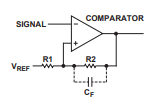
Configuring the AD8561 with Hysteresis
Hysteresis Configuration
In this setup, the input signal is applied directly to the noninverting input of the comparator. The output is then fed back to the inverting input through resistors R1 and R2. The ratio of R1 to (R1 + R2) determines the width of the hysteresis window, while VREF sets the center point, or the average switching voltage.
- The output switches high when the input voltage rises above VHI.
- It switches low only when the input voltage falls below VLO, as defined by Equation 1:VHI=(R1R1+R2)(V+−VREF)+VREFV_{HI} = \left(\frac{R1}{R1 + R2}\right)(V^+ - V_{REF}) + V_{REF}VHI=(R1+R2R1)(V+−VREF)+VREFVLO=VREF(1−R1R1+R2)V_{LO} = V_{REF}\left(1 - \frac{R1}{R1 + R2}\right)VLO=VREF(1−R1+R2R1)
Where V+ is the positive supply voltage.
A capacitor CF may also be added to the feedback network to introduce a pole. This increases hysteresis at higher frequencies, which is especially useful when dealing with slow signals in a noisy, high-frequency environment.
- At frequencies above:fP=12πCFR2f_P = \frac{1}{2\pi C_F R2}fP=2πCFR21
the hysteresis window expands, approaching VHI = V+ – 1 V and VLO = 0 V.
- At frequencies below fP, the switching thresholds remain as defined by Equation 1.
Conclusion
By applying positive feedback with resistors R1 and R2, the AD8561 can be configured with a controllable hysteresis window, improving stability in noisy environments. The reference voltage (VREF) defines the switching center, while resistor ratios set the window size. Adding a capacitor (CF) further enhances high-frequency noise immunity, ensuring reliable switching performance across a wide range of operating conditions.

Christopher Anderson
Christopher Anderson has a Ph.D. in electrical engineering, focusing on power electronics. He’s been a Senior member of the IEEE Power Electronics Society since 2021. Right now, he works with the KPR Institute of Engineering and Technology in the U.S. He also writes detailed, top-notch articles about power electronics for business-to-business electronics platforms.
Subscribe to JMBom Electronics !


