


AD8564 Comparator Stability with Hysteresis
Catalog
Product OverviewKey FeaturesTypical ApplicationsPIN CONFIGURATIONSSpecificationsApplicationsUsing HysteresisOUTLINE DIMENSIONSConclusionProduct Overview
The AD8564 is a quad-channel comparator with a fast 7 ns response time. It features separate input and output power supplies, allowing the input stage to operate from either ±5 V dual supplies or a single 5 V supply, while still delivering CMOS-/TTL-compatible outputs.
With its 7 ns propagation delay, the AD8564 is well-suited for timing applications and line receiver designs. The use of independent analog and digital power supplies helps minimize interference between supply pins. Pin-compatible with the MAX901, the AD8564 also offers lower supply current consumption.
Each of the four comparators provides consistent performance, with nearly identical propagation delays for both rising and falling edges, maintaining stability across temperature and voltage variations. These features make the AD8564 an excellent choice for high-speed timing and data communication systems. For applications needing a single comparator with a latch function, see the AD8561.
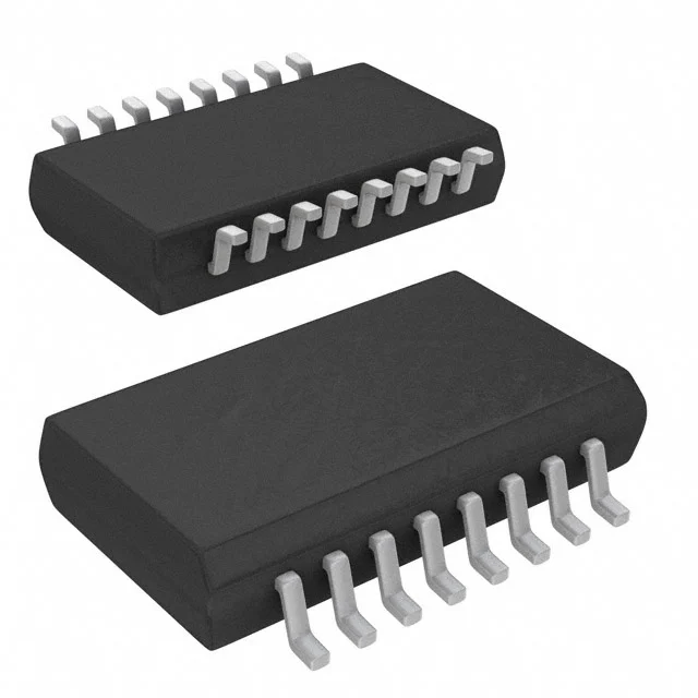
The AD8564 is specified for operation across the industrial temperature range (−40°C to +125°C) and is available in three package options: 16-lead TSSOP, 16-lead narrow-body SOIC, and 16-lead plastic DIP.
Key Features
- Operates from a single 5 V supply
- Ultra-fast 7 ns propagation delay
- Low power consumption
- Independent input and output power sections
- TTL/CMOS logic-compatible outputs
- Wide output voltage swing
- Available in TSSOP, SOIC, and PDIP package options
Typical Applications
- High-speed timing circuits
- Line receiver designs
- Data communication systems
- High-speed voltage-to-frequency (V-to-F) converters
- Battery-powered instruments
- High-speed sampling systems
- Window comparator designs
- PCMCIA card applications
- Direct replacement for MAX901-based designs
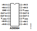
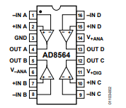
PIN CONFIGURATIONS
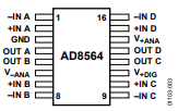
16-Lead TSSOP
(RU-16)
16-Lead Narrow Body SOIC
(R-16)
16-Lead PDIP
(N-16)
Specifications
Electrical Characteristics
(Conditions: V+ANA = V+DIG = 5.0 V, V−ANA = 0 V, TA = 25°C, unless otherwise noted.)
| Parameter | Symbol | Test Conditions | Min | Typ | Max | Unit |
|---|---|---|---|---|---|---|
| Input Characteristics | ||||||
| Offset Voltage | VOS | — | 2.3 | — | 7 | mV |
| Offset Voltage (−40°C to +125°C) | — | — | — | — | 8 | mV |
| Offset Voltage Drift | ΔVOS/ΔT | — | — | 4 | — | μV/°C |
| Input Bias Current | IB | VCM = 0 V | ±4 | — | — | μA |
| Input Bias Current (−40°C to +125°C) | — | — | ±9 | — | — | μA |
| Input Offset Current | IOS | VCM = 0 V | ±3 | — | — | μA |
| Input Common-Mode Voltage Range | VCM | — | 0 | — | 2.75 | V |
| Common-Mode Rejection Ratio | CMRR | 0 V ≤ VCM ≤ 3.0 V | 65 | — | 85 | dB |
| Large-Signal Voltage Gain | AVO | RL = 10 kΩ | 3000 | — | — | V/V |
| Input Capacitance | CIN | — | — | 3.0 | — | pF |
| Digital Outputs | ||||||
| Logic High Voltage | VOH | IOH = −3.2 mA, ΔVIN > 250 mV | 2.4 | — | 3.5 | V |
| Logic Low Voltage | VOL | IOL = 3.2 mA, VIN > 250 mV | 0.3 | — | 0.4 | V |
| Dynamic Performance | ||||||
| Propagation Delay | tP | 200 mV step, 100 mV overdrive | 6.75 | — | 9.8 | ns |
| Propagation Delay (−40°C to +125°C) | — | — | — | — | 13 | ns |
| Propagation Delay | — | 100 mV step, 5 mV overdrive | — | 8 | — | ns |
| Differential Propagation Delay (Rise vs. Fall) | ΔtP | 100 mV step, 20 mV overdrive | 0.5 | — | 2.0 | ns |
| Rise Time | — | 20% to 80% | — | 3.8 | — | ns |
| Fall Time | — | 20% to 80% | — | 1.5 | — | ns |
| Power Supply | ||||||
| Power Supply Rejection Ratio | PSRR | 4.5 V ≤ V+ANA and V+DIG ≤ 5.5 V | 80 | — | — | dB |
| Analog Supply Current | I+ANA | — | 10.5 | — | 14.0 | mA |
| Analog Supply Current (−40°C to +85°C) | — | — | — | — | 15.6 | mA |
| Analog Supply Current (−40°C to +125°C) | — | — | — | — | 17 | mA |
| Digital Supply Current | IDIG | VO = 0 V, RL = ∞ | 6.0 | — | 7.0 | mA |
| Digital Supply Current (−40°C to +125°C) | — | — | — | — | 8.0 | mA |
| Negative Analog Supply Current | I−ANA | — | –7.0 | — | +14.0 | mA |
| Negative Analog Supply Current (−40°C to +85°C) | — | — | — | — | 15.6 | mA |
| Negative Analog Supply Current (−40°C to +125°C) | — | — | — | — | 17 | mA |
Electrical Specifications
(Conditions: V+ANA = V+DIG = 5.0 V, V−ANA = 0 V, TA = 25°C, unless otherwise noted.)
| Parameter | Symbol | Test Conditions | Min | Typ | Max | Unit |
|---|---|---|---|---|---|---|
| Input Characteristics | ||||||
| Offset Voltage | VOS | — | 2.3 | — | 7 | mV |
| Offset Voltage (−40°C to +125°C) | — | — | — | — | 10 | mV |
| Offset Voltage Drift | ΔVOS/ΔT | — | — | 4 | — | μV/°C |
| Input Bias Current | IB | VCM = 0 V | ±4 | — | — | μA |
| Input Bias Current (−40°C to +125°C) | — | — | ±9 | — | — | μA |
| Input Offset Current | IOS | VCM = 0 V | ±3 | — | — | μA |
| Input Common-Mode Voltage Range | VCM | — | −4.9 | — | +3.5 | V |
| Common-Mode Rejection Ratio | CMRR | 0 V ≤ VCM ≤ 3.0 V | 65 | — | 85 | dB |
| Large-Signal Voltage Gain | AVO | RL = 10 kΩ | 3000 | — | — | V/V |
| Input Capacitance | CIN | — | — | 3.0 | — | pF |
| Digital Outputs | ||||||
| Logic High Voltage | VOH | IOH = –3.2 mA, ΔVIN > +250 mV | 2.6 | — | 3.6 | V |
| Logic Low Voltage | VOL | IOL = 3.2 mA, ΔVIN > 250 mV | 0.2 | — | 0.3 | V |
| Dynamic Performance | ||||||
| Propagation Delay | tP | 200 mV step, 100 mV overdrive | 6.75 | — | 9.8 | ns |
| Propagation Delay (−40°C to +85°C) | — | — | 8 | — | 13 | ns |
| Propagation Delay | — | 100 mV step, 5 mV overdrive | — | 8 | — | ns |
| Differential Propagation Delay (Rise vs. Fall) | ΔtP | 100 mV step, 20 mV overdrive | 0.5 | — | 2.0 | ns |
| Rise Time | — | 20% to 80% | — | 3 | — | ns |
| Fall Time | — | 20% to 80% | — | 3 | — | ns |
| Power Supply | ||||||
| Power Supply Rejection Ratio | PSRR | 4.5 V ≤ V+ANA and V+DIG ≤ 5.5 V | 50 | — | 70 | dB |
| Analog Supply Current | I+ANA | — | 10.8 | — | 14.0 | mA |
| Analog Supply Current (−40°C to +85°C) | — | — | — | — | 15.6 | mA |
| Analog Supply Current (−40°C to +125°C) | — | — | — | — | 17 | mA |
| Digital Supply Current | IDIG | VO = 0 V, RL = ∞ | 3.6 | — | 4.4 | mA |
| Digital Supply Current (−40°C to +125°C) | — | — | — | — | 5.6 | mA |
| Negative Analog Supply Current | I−ANA | — | −8.2 | — | +14.0 | mA |
| Negative Analog Supply Current (−40°C to +85°C) | — | — | — | — | 15.6 | mA |
| Negative Analog Supply Current (−40°C to +125°C) | — | — | — | — | 17 | mA |
Absolute Maximum Ratings
| Parameter | Rating |
|---|---|
| Total Analog Supply Voltage | 14 V |
| Digital Supply Voltage | 17 V |
| Analog Positive Supply to Digital Positive Supply | –600 mV |
| Input Voltage¹ | ±7 V |
| Differential Input Voltage | ±8 V |
| Output Short-Circuit Duration to GND | Indefinite |
| Storage Temperature Range | –65°C to +150°C |
| Operating Temperature Range | –55°C to +125°C |
| Junction Temperature Range | –65°C to +150°C |
| Lead Temperature Range (Soldering, 10 sec) | 300°C |
Applications
Optimizing High-Speed Performance
Like any high-speed comparator or amplifier, the AD8564 requires careful design and PCB layout to achieve its best performance. Limitations in high-speed circuits often come from stray capacitance, poor ground impedance, or other layout-related issues.
One key factor is minimizing source resistance at the input. High source resistance, when combined with the device’s input capacitance, can slow down the input response and delay the output. The AD8564 input capacitance, together with parasitic capacitance to ground, can add up to several picofarads. For example, a 3 kΩ source resistance with 5 pF of capacitance creates a 15 ns time constant—slower than the AD8564’s 5 ns capability. For optimal performance, keep source impedance below 1 kΩ.
Power supply decoupling is also critical in high-speed applications. Place a 1 μF electrolytic bypass capacitor within 0.5 inches of each power pin to ground to help filter supply ripple. In addition, place a 10 nF ceramic capacitor as close as possible to each supply pin to provide a fast local charge reservoir during high-frequency switching.
Using a solid ground plane is strongly recommended. A continuous conductive plane across the PCB, with openings only where necessary for current paths, provides a low-inductance ground. This minimizes ground bounce and eliminates potential differences between ground points. A proper ground plane also reduces the effects of stray capacitance, further improving high-speed operation.
Output Loading Considerations
The AD8564 output stage can source or sink up to 40 mA without noticeably affecting propagation delay. However, the output should not be connected to more than 20 TTL logic inputs or used to drive a load resistance below 100 Ω.
For best performance, minimize capacitive loading at the output. Capacitive loads greater than 50 pF may cause ringing on the output waveform and reduce the comparator’s bandwidth. Propagation delay also increases when capacitive loading exceeds 100 pF.
Input Stage and Bias Currents
The AD8564 employs a PNP differential input stage, allowing the common-mode input voltage to extend from the negative supply rail up to within about 2.2 V of the positive supply rail. The common-mode voltage is defined as the average of the two input voltages. For the fastest response, the input common-mode voltage should stay within this range.
The typical input bias current is 4 μA. With a PNP input stage, this current goes to zero on a high input and doubles on a low input. Therefore, when using large-value resistors at the inputs, care must be taken to avoid significant voltage drops caused by this bias current.
The typical input capacitance is 3 pF. This value can be determined by applying a large source resistance to the input and measuring the resulting change in propagation delay.
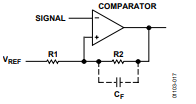
Using Hysteresis
Hysteresis can be introduced into a comparator by applying positive feedback. This technique is especially useful in noisy environments, where it helps prevent the output from rapidly toggling between states when the input signal is close to the switching threshold.
Figure 17 illustrates a typical configuration of the AD8564 with hysteresis added.
Configuring the AD8564 with Hysteresis
Using Hysteresis
Hysteresis can be introduced into a comparator by applying positive feedback. This technique is especially useful in noisy environments, where it helps prevent the output from rapidly toggling between states when the input signal is close to the switching threshold.
Picture illustrates a typical configuration of the AD8564 with hysteresis added.
Where V+ represents the positive supply voltage.
An optional capacitor (CF) can be added to the feedback network to introduce a pole. This increases the hysteresis at higher frequencies, which is especially useful when evaluating relatively slow signals in environments with significant high-frequency noise.
For frequencies abovefP=12πR2CF,f_P = \frac{1}{2 \pi R_2 C_F},fP=2πR2CF1,
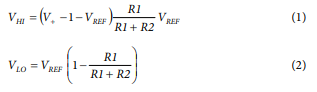
the hysteresis window shifts toward VHI = V+ – 1 V and VLO = 0 V.
For frequencies below fP, the switching thresholds remain as defined in Equation 1.
OUTLINE DIMENSIONS
![16-Lead Plastic Dual In-Line Package [PDIP] (N-16) Dimensions shown in inches and (millimeters)](https://res.jmbom.com/upload/2025/9/1758091653781719.webp)
16-Lead Plastic Dual In-Line Package [PDIP]
(N-16)
Dimensions shown in inches and (millimeters)
![16-Lead Standard Small Outline Package [SOIC_N] Narrow Body (R-16) Dimensions shown in millimeters and (inches)](https://res.jmbom.com/upload/2025/9/1758091709255272.webp)
16-Lead Standard Small Outline Package [SOIC_N]
Narrow Body
(R-16)
Dimensions shown in millimeters and (inches)
![16-Lead Thin Shrink Small Outline Package [TSSOP] (RU-16) Dimensions shown in millimeters](https://res.jmbom.com/upload/2025/9/1758091751458942.webp)
16-Lead Thin Shrink Small Outline Package [TSSOP]
(RU-16)
Dimensions shown in millimeters
Conclusion
Adding hysteresis to the AD8564 using positive feedback, and optionally including a CF capacitor, improves noise immunity by stabilizing the output near the switching threshold. The CF capacitor allows the hysteresis effect to increase at higher frequencies, making the comparator more reliable when monitoring slow signals in noisy, high-frequency environments. Threshold voltages adjust depending on the signal frequency relative to the feedback pole, ensuring predictable switching behavior.

Christopher Anderson
Christopher Anderson has a Ph.D. in electrical engineering, focusing on power electronics. He’s been a Senior member of the IEEE Power Electronics Society since 2021. Right now, he works with the KPR Institute of Engineering and Technology in the U.S. He also writes detailed, top-notch articles about power electronics for business-to-business electronics platforms.
Subscribe to JMBom Electronics !


