


PCAL6416A Low-Voltage 16-Bit I²C I/O Expander Overview
Catalog
General DescriptionFeatures and Benefits Ordering Information Block diagram of PCAL6416APinning informationFunctional descriptionConclusionGeneral Description
The PCAL6416A is a 16-bit general-purpose I/O expander designed to extend the I/O capabilities of most microcontroller families through an I²C-bus interface.NXP’s I/O expanders offer a simple and efficient solution for adding extra I/O lines while minimizing wiring complexity—ideal for battery-powered mobile devices that need to connect with sensors, keypads, or push buttons.
Beyond offering flexible GPIO options, the PCAL6416A makes it easier to connect processors and peripherals that operate at different voltage levels. Its built-in level shifting allows smooth communication in mixed-voltage environments, ensuring compatibility between low-voltage processors and higher-voltage I/O devices.
With a wide operating voltage range of 1.65 V to 5.5 V, the PCAL6416A supports seamless communication between next-generation microcontrollers (on the I²C side, SDA/SCL) and peripherals (on the port side).
The device operates with two separate supply voltages:
- VDD(I²C-bus) powers the I²C interface on the master side (e.g., a microcontroller).
- VDD(P) powers the internal circuits and Port P.
Voltage level translation is handled through VDD(I²C-bus), which should match the voltage level of the external SCL/SDA lines. This setup defines the I²C bus voltage, while VDD(P) determines the voltage level of Port P.
The PCAL6416A includes the same register set as the PCA6416A—four pairs of 8-bit registers for Configuration, Input, Output, and Polarity Inversion—but also features Agile I/O enhancements. These added functions include:
- Programmable output drive strength
- Latchable inputs
- Programmable pull-up/pull-down resistors
- Maskable interrupt capability
- Interrupt status register
- Selectable open-drain or push-pull outputs
The PCAL6416A is pin-to-pin compatible with the PCA6416A, but it initializes with all I/O interrupts masked by default. This prevents unwanted interrupts during board startup and simplifies system bring-up.
On power-up, all I/Os are configured as inputs. The system master can later configure each pin as either an input or output by writing to the appropriate configuration bits. Input and output data are stored in their respective registers, and input polarity can be inverted using the Polarity Inversion register, eliminating the need for external logic gates. The integrated programmable pull-up and pull-down resistors further reduce the need for extra components.
If a timeout or malfunction occurs, the system master can reset the PCAL6416A by pulling the RESET pin LOW. A power-on reset restores all registers to their default settings and reinitializes the I²C/SMBus state machine. Using the RESET pin achieves the same result without needing to power-cycle the device.
Low-Voltage Translating 16-Bit I²C-Bus/SMBus I/O Expander with Interrupt Output, Reset, and Configuration Registers
The PCAL6416A features a low-voltage, 16-bit I²C/SMBus I/O expander equipped with interrupt output, reset control, and configuration registers for flexible system integration.
The device includes an open-drain interrupt (INT) output that is triggered whenever an input’s state changes compared to its corresponding value in the Input Port register. This signal notifies the system master of input changes without the need for continuous polling over the I²C bus.
The INT pin can be connected directly to a microcontroller’s interrupt input. When activated, it alerts the microcontroller that one or more input states have changed, allowing the system to respond immediately—while the PCAL6416A remains a simple slave device on the I²C bus.
To ensure reliable detection, the input latch feature captures and holds the pin states that caused the interrupt until the master reads and clears the interrupt. This helps prevent missed events, even with rapidly changing input signals, and reduces the host’s interrupt service load.
Each Port P output can sink up to 25 mA, enabling direct LED drive capability with low overall current consumption.
Additionally, the ADDR pin allows for easy hardware configuration of the I²C address, enabling up to two PCAL6416A devices to operate on the same I²C or SMBus for expanded system flexibility.
Features and Benefits
• I²C-bus to parallel port expander for easy GPIO extension
• Wide operating voltage range: 1.65 V to 5.5 V
• Supports bidirectional voltage-level translation and GPIO expansion between different voltage domains:
– 1.8 V SCL/SDA and 1.8 V / 2.5 V / 3.3 V / 5 V Port P
– 2.5 V SCL/SDA and 1.8 V / 2.5 V / 3.3 V / 5 V Port P
– 3.3 V SCL/SDA and 1.8 V / 2.5 V / 3.3 V / 5 V Port P
– 5 V SCL/SDA and 1.8 V / 2.5 V / 3.3 V / 5 V Port P
• Ultra-low standby current:
– 1.5 μA typical at 5 V VDD
– 1.0 μA typical at 3.3 V VDD
• Schmitt trigger inputs on SCL and SDA provide reliable operation with slow signal transitions and improved noise immunity
– Typical hysteresis: 0.18 V (1.8 V), 0.25 V (2.5 V), 0.33 V (3.3 V), 0.5 V (5 V)
• 5 V-tolerant I/O ports for enhanced compatibility
• Active LOW reset (RESET) input for easy device initialization
• Open-drain active LOW interrupt (INT) output for flexible system signaling
• Supports up to 400 kHz Fast-mode I²C communication
• Built-in power-on reset ensures proper startup behavior
• All channels default to input mode at power-up
• Glitch-free startup for stable operation
• Integrated noise filter on SCL and SDA lines for cleaner signal integrity
• Latched outputs capable of driving up to 25 mA, ideal for direct LED control
• Latch-up performance exceeds 100 mA per JESD78, Class II standard
• Excellent ESD protection per JESD22 standards:
– 2000 V Human Body Model (A114-A)
– 1000 V Charged Device Model (C101)
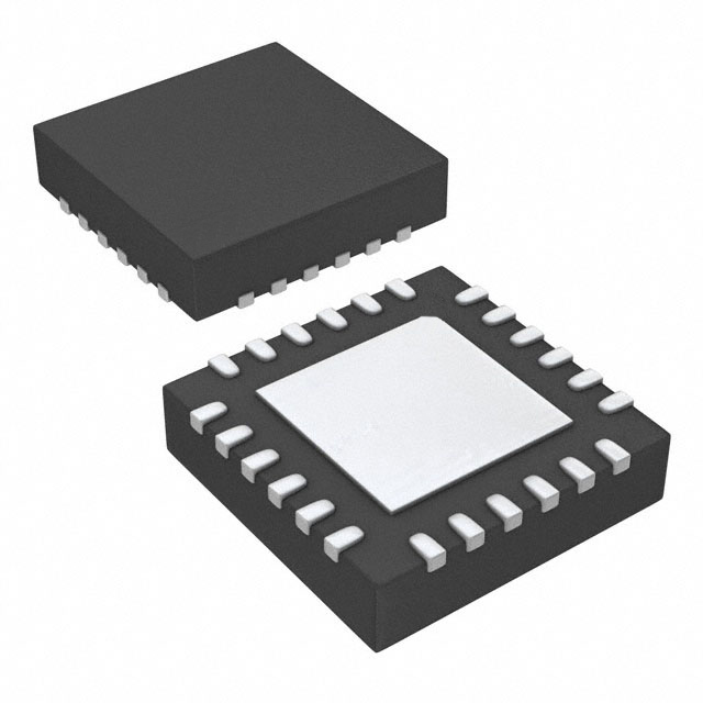
• Available in multiple compact package options: TSSOP24, HWQFN24, VFBGA24, and X2QFN24 (LGA type)
Low-Voltage Translating 16-Bit I²C-Bus/SMBus I/O Expander with Interrupt Output, Reset, and Configuration Registers
2.1 Agile I/O Features
• Software compatible with PCA6416A, ensuring seamless integration, with interrupts disabled by default at power-up
• Pin-to-pin drop-in replacement for PCA6416A—no hardware redesign needed
• Configurable output ports: each port bank can be set to push-pull or open-drain output mode for design flexibility
• Interrupt status register: read-only register clearly indicates which input triggered an interrupt
• Bit-level I/O configuration options provide greater control and flexibility:
– Programmable output drive strength: four selectable drive levels to optimize rise and fall times, especially in low-capacitance circuits
– Input latch function: stores input state changes until the Input Port register is read, ensuring no missed transitions
– Pull-up/pull-down resistor control: allows floating inputs or enables internal pull-up/pull-down resistors as needed
– Selectable resistor type: choose between 100 kΩ pull-up or pull-down resistors for input stability
– Interrupt masking: prevents unwanted interrupt generation from input state changes, reducing false triggers and improving system stability
Ordering Information
| Type Number | Topside Marking | Package Name | Description | Version |
|---|---|---|---|---|
| PCAL6416AEV | L16A | VFBGA24 | Plastic very thin fine-pitch ball grid array package, 24 balls; body size 3 × 3 × 0.85 mm | SOT1199-1 |
| PCAL6416AEX1 | 16X111 | X2QFN24 | Plastic, thermally enhanced super thin land grid array or quad flat package; no leads; 24 terminals; body size 2.0 × 2.0 × 0.35 mm | SOT1895-1 |
| PCAL6416AHF | L16A | HWQFN24 | Plastic, thermally enhanced ultra-thin quad flat package; no leads; 24 terminals; body size 4 × 4 × 0.75 mm | SOT994-1 |
| PCAL6416APW | PCAL6416A | TSSOP24 | Plastic thin shrink small outline package; 24 leads; body width 4.4 mm | SOT355-1 |
Table 1. Ordering Information
111 “X” varies from 1 to 5 and represents the work week within the specified month.
3.1 Ordering Options
| Type Number | Orderable Part Number | Package | Packing Method | Minimum Order Quantity | Temperature Range |
|---|---|---|---|---|---|
| PCAL6416AEV | PCAL6416AEVJ | VFBGA24 | 13" reel (Q1/T1) – Standard SMD marking | 6000 | –40 °C to +85 °C |
| PCAL6416AEX1 | PCAL6416AEX1Z | X2QFN24 | 7" reel (Q2/T3) – Standard SMD marking | 5000 | –40 °C to +85 °C |
| PCAL6416AHF | PCAL6416AHF,128 | HWQFN24 | 13" reel (Q2/T3) – Standard SMD marking | 6000 | –40 °C to +85 °C |
| PCAL6416APW | PCAL6416APW,118 | TSSOP24 | 13" reel (Q1/T1) – Standard SMD marking | 2500 | –40 °C to +85 °C |
Block diagram of PCAL6416A
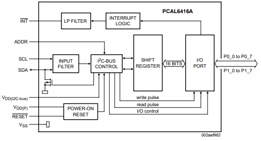
All I/Os are set to inputs at reset.
Figure 1. Block diagram of PCAL6416A (positive logic)
Pinning information
5.1 Pinning
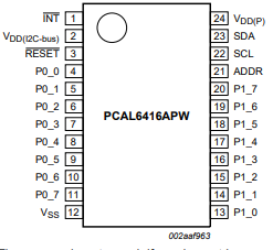
Figure 2. Pin configuration for TSSOP24
The exposed center pad, if used, must be connected only as a secondary ground or must be left electrically open.
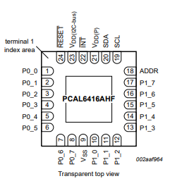
Figure 3. Pin configuration for HWQFN24
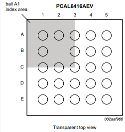
Figure 4. Pin configuration for VFBGA24 (3mm × 3 mm)
An empty cell indicates no ball is populated at that grid point.
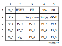
Figure 5. Ball mapping for VFBGA24 (3 mm× 3 mm) (transparent top view)
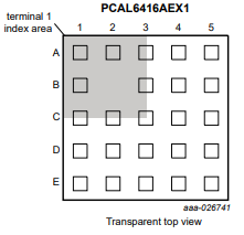
Figure 6. Pin configuration for X2QFN24 (2mm × 2 mm); EX1 land grid array option
An empty cell indicates no ball is populated at that grid point.
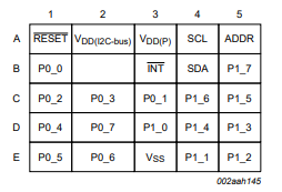
Figure 7. Ball mapping for X2QFN24 (2 mm × 2 mm) (transparent top view)
5.2 Pin Description (Rewritten in natural, customer-friendly English)
| Symbol | Pin Number | Description |
|---|---|---|
| TSSOP24 | HWQFN24 | |
| INT | 1 | 22 |
| VDD(I²C-bus) | 2 | 23 |
Functional description
Device address
The address of the PCAL6416A is shown in Figure 8
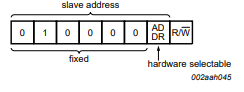
Figure 8. PCAL6416A address
ADDR is the hardware address package pin and is held to either HIGH (logic 1) or LOW (logic 0) to assign one of the two possible slave addresses. The last bit of the slave address (R/W) defines the operation (read or write) to be performed. A HIGH (logic 1) selects a read operation, while a LOW (logic 0) selects a write operation.
Conclusion
The PCAL6416A is a versatile 16-bit I²C-bus/SMBus I/O expander designed to simplify system design and enhance flexibility in mixed-voltage environments. With its wide operating voltage range (1.65 V–5.5 V), built-in level shifting, and Agile I/O features, it enables seamless communication between low-voltage processors and higher-voltage peripherals.
Its programmable drive strength, pull-up/pull-down control, interrupt management, and latchable inputs make it ideal for complex embedded applications that demand efficient I/O management and reliable signal handling. The low standby current, high ESD protection, and multiple compact package options ensure dependable performance across a wide range of operating conditions.
Overall, the PCAL6416A delivers a robust, power-efficient, and easy-to-integrate solution for expanding GPIO resources while maintaining strong compatibility with existing designs such as the PCA6416A.

Christopher Anderson
Christopher Anderson has a Ph.D. in electrical engineering, focusing on power electronics. He’s been a Senior member of the IEEE Power Electronics Society since 2021. Right now, he works with the KPR Institute of Engineering and Technology in the U.S. He also writes detailed, top-notch articles about power electronics for business-to-business electronics platforms.
Subscribe to JMBom Electronics !


