


100BASE-TX Transmit Data Flow
Catalog
GENERAL DESCRIPTIONHighlightsApplicationsLAN8700/LAN8700i System Block DiagramLAN8700/LAN8700I ARCHITECTURAL OVERVIEWPIN CONFIGURATIONLAN8700/LAN8700i 36-Pin QFN PinoutMII SIGNALSGENERAL SIGNALSARCHITECTURE DETAILS100BASE-TX DATA PATHConclusionGENERAL DESCRIPTION
The Microchip LAN8700/LAN8700i is a low-power, industrial-grade (LAN8700i) analog interface IC designed for high-performance embedded Ethernet applications. It features variable I/O voltage and HP Auto-MDIX support. The LAN8700/LAN8700i can run from a single 3.3V supply thanks to its built-in 3.3V-to-1.8V linear regulator. For systems that already provide a 1.8V power plane, the linear regulator can be disabled to streamline the design.
100BASE-TX Transmit Data Flow
Architectural Overview
The LAN8700/LAN8700i integrates an encoder/decoder, scrambler/descrambler, wave-shaping transmitter, output driver, and a twisted-pair receiver with adaptive equalization and baseline wander (BLW) correction, along with clock and data recovery capabilities. It can be set up to work with either the Media Independent Interface (MII) or the Reduced Media Independent Interface (RMII).
This device meets IEEE 802.3-2005 standards (MII pins are tolerant up to 3.6V) and supports both standard and vendor-specific register functions. It includes a full-duplex 10BASE-T/100BASE-TX transceiver, supporting 10 Mbps (10BASE-T) on Category 3 or 5 unshielded twisted-pair cables, and 100 Mbps (100BASE-TX) on Category 5 unshielded twisted-pair cables.
Highlights
- Single-chip Ethernet Physical Layer Transceiver (PHY)
- ESD protection: ±8 kV HBM without external components
- Meets EN/IEC61000-4-2 ESD standards: ±8 kV contact, ±15 kV air discharge (tested independently)
- flexPWR® Technology for flexible power management
- LVCMOS I/O voltage range: 1.6 V to 3.6 V
- Built-in 3.3 V to 1.8 V regulator for optional single-supply operation; can be disabled if 1.8 V system supply is present
- Supports HP Auto-MDIX per IEEE 802.3ab
- Supports cable lengths over 150 meters
- Automatic polarity correction
- Latch-up tolerance exceeds 150 mA (per EIA/JESD 78, Class II)
- Energy detect and low-power standby modes
- Low operating current: 39 mA typical at 10BASE-T, 79 mA typical at 100BASE-TX
- Supports auto-negotiation and parallel detection
- Compatible with MII and RMII interfaces
- Compliant with IEEE 802.3-2005 standards; MII pins tolerate up to 3.6 V
- Supports standard and vendor-specific register functions
- Integrated DSP with adaptive equalizer
- Baseline wander (BLW) correction
- Low-profile 36-pin QFN RoHS-compliant package (6 × 6 × 0.9 mm)
- 4 LED status indicators
- Commercial temperature range: 0°C to 70°C
- Industrial temperature range: -40°C to 85°C (LAN8700i)
Applications
- Set-top boxes
- Network printers and servers
- LAN-on-motherboard solutions
- 10/100 PCMCIA and CardBus devices
- Embedded telecom systems
- Video recording and playback systems
- Cable modems and routers
- DSL modems and routers
- Digital video recorders (DVRs)
- Personal video recorders (PVRs)
- IP phones and video phones
- Wireless access points
- Digital televisions (DTVs)
- Digital media adapters and media servers
- Point-of-sale (POS) terminals
- Automotive networking systems
- Gaming consoles
- Security and surveillance systems
- Power over Ethernet (PoE) applications
- Access control systems
LAN8700/LAN8700i System Block Diagram
Hubs and switches with multiple integrated MACs and external PHYs often require a high pin count due to the number of pins needed for each MII interface, which can increase overall system cost.
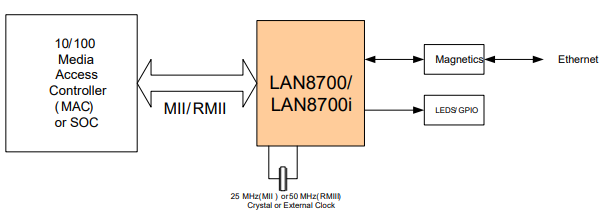
LAN8700/LAN8700i System Block Diagram
The RMII interface is designed for switch-based ASICs or other embedded solutions where minimizing pin count is critical for Ethernet connectivity. RMII uses only 6 pins per MAC-to-PHY connection, plus a single shared reference clock, compared with 16 pins required by the MII interface.
The Microchip LAN8700/LAN8700i supports operation in RMII mode. For the latest RMII specifications, please contact your Microchip sales representative.
Throughout this document, references to the LAN8700/LAN8700i apply to both commercial and industrial temperature versions, whereas the LAN8700i specifically denotes the industrial temperature variant.
LAN8700/LAN8700I ARCHITECTURAL OVERVIEW
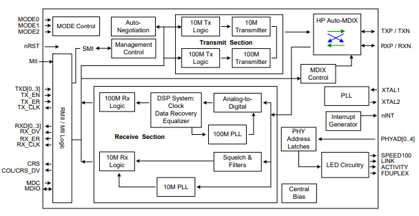
LAN8700/LAN8700I ARCHITECTURAL OVERVIEW
PIN CONFIGURATION
LAN8700/LAN8700i Package Pin-out Diagram and Signal Table
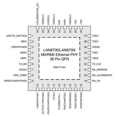
LAN8700/LAN8700i Package Pin-out Diagram and Signal Table
LAN8700/LAN8700i 36-Pin QFN Pinout
| Pin No. | Pin Name | Pin No. | Pin Name |
|---|---|---|---|
| 1 | nINT / TX_ER / TXD4 | 19 | RX_DV |
| 2 | MDC | 20 | RX_CLK / REGOFF |
| 3 | CRS / PHYAD4 | 21 | RX_ER / RXD4 |
| 4 | MDIO | 22 | TXCLK |
| 5 | nRST | 23 | TXD0 |
| 6 | TX_EN | 24 | TXD1 |
| 7 | VDD33 | 25 | VDDIO |
| 8 | VDD_CORE | 26 | TXD2 |
| 9 | SPEED100 / PHYAD0 | 27 | TXD3 |
| 10 | LINK / PHYAD1 | 28 | TXN |
| 11 | ACTIVITY / PHYAD2 | 29 | TXP |
| 12 | FDUPLEX / PHYAD3 | 30 | VDDA3.3 |
| 13 | XTAL2 | 31 | RXN |
| 14 | CLKIN / XTAL1 | 32 | RXP |
| 15 | RXD3 / nINTSEL | 33 | VDDA3.3 |
| 16 | RXD2 / MODE2 | 34 | EXRES1 |
| 17 | RXD1 / MODE1 | 35 | VDDA3.3 |
| 18 | RXD0 / MODE0 | 36 | COL / RMII / CRS_DV |
PIN DESCRIPTION
This section explains the function of each pin. Signals that start with a lowercase “n” are active low. For example, nRST indicates that the reset signal is active low.
3.1 I/O Signals
The buffer types shown in the TYPE column of the tables are as follows:
- I – Input. Digital LVCMOS levels.
- IPD – Input with internal pull-down. Digital LVCMOS levels.
- O – Output. Digital LVCMOS levels.
- OPD – Output with internal pull-down. Digital LVCMOS levels.
- I/O – Input or output. Digital LVCMOS levels.
- IOPD – Input or output with internal pull-down. Digital LVCMOS levels.
- IOPU – Input or output with internal pull-up. Digital LVCMOS levels.
- AI – Analog input.
- AO – Analog output.
Note: Digital signals are not 5V tolerant. The voltage range is 1.6V to 3.6V.
MII SIGNALS
| Signal Name | Type | Description |
|---|---|---|
| TXD0 | I | Transmit Data 0: Bit 0 of the 4 data bits sent to the PHY. |
| TXD1 | I | Transmit Data 1: Bit 1 of the 4 data bits sent to the PHY. |
| TXD2 | I | Transmit Data 2: Bit 2 of the 4 data bits sent to the PHY. Note: Ground this pin in RMII mode. |
| TXD3 | I | Transmit Data 3: Bit 3 of the 4 data bits sent to the PHY. Note: Ground this pin in RMII mode. |
| nINT / TX_ER / TXD4 | IOPU | MII Transmit Error: Driving high substitutes the Transmit Error code (/H/) for the encoded data. Ignored in 10BASE-T. MII Transmit Data 4: In 5B Symbol Interface mode, this becomes the MSB of the 5-bit symbol code-group. Notes: - Not used in RMII mode - Multiplexed with nINT - See Section 4.10 for strapping options. |
| TX_EN | IPD | Transmit Enable: Signals that valid data is on TXD[3:0] for transmission. Note: In RMII mode, only TXD[1:0] are valid. |
| TX_CLK | O | Transmit Clock: 25 MHz for 100BASE-TX, 2.5 MHz for 10BASE-T. Notes: - Not used in RMII mode - For proper TXCLK operation, RX_ER and RX_DV must not be externally driven high during hardware reset or power-up. |
MII Receive Signals
| Signal Name | Type | Description |
|---|---|---|
| RXD0 / MODE0 | IOPU | Receive Data 0: Bit 0 of the 4 data bits sent by the PHY on the receive path. PHY Operating Mode Bit 0: Sets the default PHY mode. Note: See Section 5.4.9.2, "Mode Bus – MODE[2:0]" for mode options. |
| RXD1 / MODE1 | IOPU | Receive Data 1: Bit 1 of the 4 data bits sent by the PHY on the receive path. PHY Operating Mode Bit 1: Sets the default PHY mode. Note: See Section 5.4.9.2 for mode options. |
| RXD2 / MODE2 | IOPU | Receive Data 2: Bit 2 of the 4 data bits sent by the PHY on the receive path. PHY Operating Mode Bit 2: Sets the default PHY mode. Notes: - RXD2 is not used in RMII mode. - See Section 5.4.9.2 for mode options. |
| RXD3 / nINTSEL | IOPU | Receive Data 3: Bit 3 of the 4 data bits sent by the PHY. nINTSEL: Determines the function of the nINT/TX_ER/TXD4 pin at power-up or after external reset. Configuration: - Floating or pulled to VDDIO → nINT is selected (default). - Pulled low to VSS via resistor → TX_ER/TXD4 is selected. Notes: - RXD3 is not used in RMII mode. - If nINT mode is selected, a pull-up resistor to VDDIO is required. - See Section 4.10 for detailed strapping options. |
| RX_ER / RXD4 | OPD | Receive Error: Asserted to indicate an error in the current frame from the PHY. MII Receive Data 4: In 5B Symbol Interface mode, this pin becomes the MSB of the 5-bit symbol code-group. Otherwise, it functions as RX_ER. Notes: - Has internal pull-down resistor; must not be high during reset. - RX_ER is optional in RMII mode. |
| RX_DV | O | Receive Data Valid: Indicates that decoded data nibbles are presented on RXD[3:0]. Notes: - Has internal pull-down resistor; must not be high during reset. - Not used in RMII mode. |
MII / RMII Signals
| Signal Name | Type | Description |
|---|---|---|
| RX_CLK / REGOFF | IOPD | Receive Clock (RX_CLK): In MII mode, outputs the receive clock. 25 MHz for 100BASE-TX, 2.5 MHz for 10BASE-T. Note: Not used in RMII mode. Regulator Off (REGOFF): Pull high to disable the internal 1.8V regulator. During power-on, this pin determines whether the internal regulator turns on. If disabled, an external 1.8V must be supplied to VDD_CORE, and VDD33 must be ≥2.64V before applying voltage to VDD_CORE. |
| COL / RMII / CRS_DV | IOPD | MII Mode Collision Detect (COL): Asserted when a collision is detected. RMII Mode: This pin selects MII or RMII mode at the rising edge of internal reset (nRESET) using strapping: - Float → MII mode - Pull-high via resistor to VDDIO → RMII mode See Section 4.6.3 for details. CRS_DV in RMII: Indicates the receive medium is active. In 10BT half-duplex, RXD[1:0] remains low until the SFD byte (10101011) is received. Transmitted data is not looped back onto RX pins. |
| CRS / PHYAD4 | IOPU | Carrier Sense: Indicates detection of carrier signal. Note: Multiplexed with PHYAD4. |
LED Signals
| Signal Name | Type | Description |
|---|---|---|
| SPEED100 / PHYAD0 | IOPU | LED1 – Speed Indicator: Active = 100 Mbps, Inactive = 10 Mbps. Note: Multiplexed with PHYAD0. |
| LINK / PHYAD1 | IOPU | LED2 – Link Status: Active indicates the link (10BASE-T or 100BASE-TX) is up. Note: Multiplexed with PHYAD1. |
| ACTIVITY / PHYAD2 | IOPU | LED3 – Activity: Active indicates carrier sense (CRS) from the active PMD. Note: Multiplexed with PHYAD2. |
| FDUPLEX / PHYAD3 | IOPU | LED4 – Duplex: Active indicates full-duplex mode. Note: Multiplexed with PHYAD3. |
Management Signals
| Signal Name | Type | Description |
|---|---|---|
| MDIO | IOPD | Management Data Input/Output: Serial management data line. |
| MDC | IPD | Management Clock: Serial management clock for MDIO interface. |
BOOT STRAP CONFIGURATION INPUTS
| Signal Name | Type | Description |
|---|---|---|
| CRS / PHYAD4 | IOPU | PHY Address Bit 4: Sets the default PHY address. Multiplexed with CRS. |
| FDUPLEX / PHYAD3 | IOPU | PHY Address Bit 3: Sets the default PHY address. Multiplexed with FDUPLEX. |
| ACTIVITY / PHYAD2 | IOPU | PHY Address Bit 2: Sets the default PHY address. Multiplexed with ACTIVITY. |
| LINK / PHYAD1 | IOPU | PHY Address Bit 1: Sets the default PHY address. Multiplexed with LINK. |
| SPEED100 / PHYAD0 | IOPU | PHY Address Bit 0: Sets the default PHY address. Multiplexed with SPEED100. |
| RXD2 / MODE2 | IOPU | PHY Operating Mode Bit 2: Sets the default PHY mode. Multiplexed with RXD2. See: Section 5.4.9.2, "Mode Bus – MODE[2:0]" for mode options. |
| RXD1 / MODE1 | IOPU | PHY Operating Mode Bit 1: Sets the default PHY mode. Multiplexed with RXD1. See: Section 5.4.9.2 for mode options. |
| RXD0 / MODE0 | IOPU | PHY Operating Mode Bit 0: Sets the default PHY mode. Multiplexed with RXD0. See: Section 5.4.9.2 for mode options. |
| COL / RMII / CRS_DV | IOPD | Digital Communication Mode: Selects PHY mode between RMII or MII. Multiplexed with Collision (MII) or CRS_DV (RMII). - Float → MII mode - Pull up to VDDIO via resistor → RMII mode See: Table 4-3 for boot strapping resistors. |
| RXD3 / nINTSEL | IOPU | nINT Pin Mode Select: Configures the function of pin 1 (nINT/TX_ER/TXD4). - Default floating → nINT (active low interrupt output). - For nINT mode, tie pin 1 to VDDIO via resistor. - Pulled low to VSS via resistor → TX_ER/TXD4 (Transmit Error or Transmit Data 4 in 5B mode). Note: For TXD4/TX_ER mode, do not tie pin 1 to VDDIO or ground. See: Table 4-3 for resistor values. |
GENERAL SIGNALS
| Signal Name | Type | Description |
|---|---|---|
| nINT / TX_ER / TXD4 | IOPU | LAN Interrupt – Active low output. Use an external pull-up resistor to 3.3V (see Table 4-3 for values). - Multiplexed with TX_ER/TXD4. - See Section 4.10 for strapping options and additional details. |
| nRST | I | External Reset input. Active low. When deasserted, mode register bits are loaded from the mode pins (see Section 5.4.9.2). |
| CLKIN / XTAL1 | I/O | Clock Input: Accepts 25 MHz or 50 MHz external clock or crystal. - MII mode: 25 MHz reference clock. - RMII mode: 50 MHz reference clock, typically also drives the RMII-compliant MAC clock input. See Section 4.10 for strapping options. |
| XTAL2 | O | Clock Output: 25 MHz crystal output. Note: Float this pin if using an external clock via CLKIN/XTAL1. |
10/100 LINE INTERFACE
| Signal Name | Type | Description |
|---|---|---|
| TXP | AO | Transmit Data Positive: Differential transmit output for 100BASE-TX or 10BASE-T to magnetics. |
| TXN | AO | Transmit Data Negative: Differential transmit output for 100BASE-TX or 10BASE-T to magnetics. |
| RXP | AI | Receive Data Positive: Differential receive input from magnetics for 100BASE-TX or 10BASE-T. |
| RXN | AI | Receive Data Negative: Differential receive input from magnetics for 100BASE-TX or 10BASE-T. |
ANALOG REFERENCES
| Signal Name | Type | Description |
|---|---|---|
| EXRES1 | AI | Connect to a 12.4 kΩ ±1% reference resistor as described in the Analog Layout Guidelines. Nominal voltage is 1.2V, dissipating ~1 mW of power. |
POWER SIGNALS
| Signal Name | Type | Description |
|---|---|---|
| VDDIO | POWER | Variable I/O Pad Power: +1.6V to +3.6V. |
| VDD33 | POWER | Core Regulator Input: +3.3V supply for internal regulation. |
| VDDA3.3 | POWER | Analog Power: +3.3V supply for analog circuitry. |
| VDD_CORE | POWER | Core Voltage: +1.8V supply for digital circuitry on-chip. Normally provided by the on-chip regulator unless the regulator is disabled via RX_CLK/REGOFF pin. Capacitor Recommendations: - Place a 0.1 µF capacitor close to this pin to ground. - If using the on-chip regulator, place a 4.7 µF ±20% capacitor with ESR <1 Ω near the pin to ground. - X5R or X7R ceramic capacitors are recommended (ESR <0.1 Ω at frequencies >10 kHz). |
| VSS | POWER | Exposed Ground Flag: Must be connected to the ground plane. |
ARCHITECTURE DETAILS
Top-Level Functional Architecture
The LAN8700/LAN8700i PHY is organized into the following functional blocks:
- 100BASE-TX Transmit and Receive: Handles all 100 Mbps data transmission and reception.
- 10BASE-T Transmit and Receive: Handles all 10 Mbps data transmission and reception.
- MII / RMII Interface: Provides connectivity to the Ethernet controller using either the standard Media Independent Interface (MII) or Reduced Media Independent Interface (RMII).
- Auto-Negotiation: Automatically determines the optimal speed and duplex mode for communication.
- Management Control: Enables reading of status registers and writing to control registers for configuration and monitoring.
100BASE-TX DATA PATH
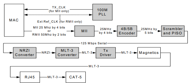
100BASE-TX DATA PATH
100BASE-TX Transmit
The 100BASE-TX transmit data path is illustrated in Figure 4-1. Key functional blocks are described below.
100M Transmit Data Across the MII/RMII Interface
- MII Mode: The MAC controller places transmit data on the TXD bus and asserts TX_EN to indicate valid data. The PHY latches the data on the rising edge of TX_CLK. The data width is 4 bits at 25 MHz.
- RMII Mode: The MAC controller drives transmit data onto the TXD bus and asserts TX_EN to indicate valid data. The PHY latches the data on the rising edge of REF_CLK. The data width is 2 bits at 50 MHz.
4B/5B Encoding
- The transmit data is passed from the MII block to the 4B/5B encoder, which converts 4-bit nibbles into 5-bit symbols (code-groups).
- Out of 32 possible code-groups, 16 represent standard data (hexadecimal 0–F), while the remaining 16 are reserved for control or invalid codes (e.g., /I/ for IDLE, /H/ for Transmit Error).
- Encoding Bypass: The 4B/5B encoding can be bypassed by clearing bit 6 of register 31. In bypass mode, the 5th transmit bit carries the TX_ER signal.
- Important: Encoding can only be bypassed when the MAC interface is operating in MII mode.
Conclusion
The 100BASE-TX transmit path ensures reliable high-speed data transfer through precise MII/RMII interfacing and robust 4B/5B encoding. Its flexible design, including the option to bypass encoding in MII mode, provides adaptability for different system requirements.

Amanda Miller
Amanda Miller is a senior electronics engineer with 6 years of experience. She focuses on studying resistors, transistors, and package design in detail. Her deep knowledge helps her bring innovation and high standards to the electronics industry.
Subscribe to JMBom Electronics !


