


74LS08 AND Gate IC:Applications,Features & FAQ
Catalog
What is the 74LS08 AND Gate IC?Pin Configuration of 74LS08Features & Specifications of 74LS08How to Use the 74LS08 AND Gate ICApplications of 74LS08Frequently Asked QuestionsFinal WordsIf we try to design a circuit manually just for a single AND gate, it can take quite a bit of time because of how large the design can get. That’s where the 74LS08 AND gate IC comes in—it’s used to make things easier. There are also other logic gate ICs in the same series, like the 74LS00, 74LS73, 74LS02, 74LS138, and 74LS04. This article gives a quick look at the 74LS08 AND gate IC and how it works.
What is the 74LS08 AND Gate IC?
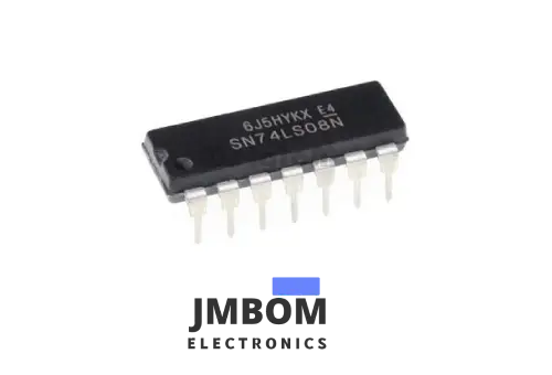
74LS08
The 74LS08 is an AND logic gate IC that has 4 separate AND gates. Each gate works on its own without affecting the others, which is why it’s called a QUADRUPLE two-input AND gate. It uses just one power supply and comes in different packages depending on what the circuit needs.
This IC is part of the 74XXYY series and is built using Schottky transistors to give it high-speed logic operations. Its output is always TTL, making it easy to work with other microcontrollers and TTL devices. The 74LS08 is also compact and performs fast, which makes it reliable for all sorts of devices.
Pin Configuration of 74LS08
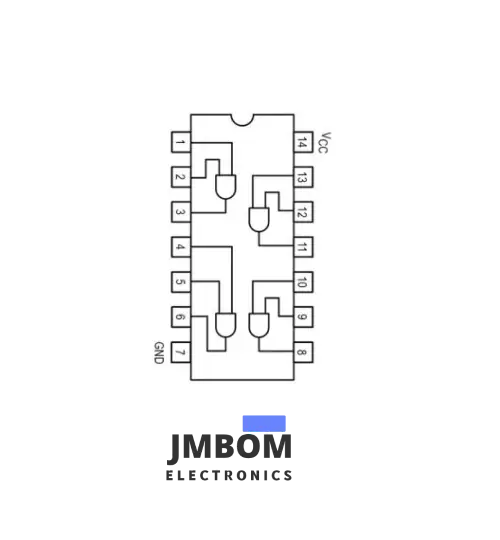
Pin Configuration of 74LS08
So, the pin configuration for the 74LS08 AND gate IC is laid out below. It has 14 pins, and here’s a quick rundown of what each one does:
- Pin 1 (A1): This is the first input for the 1st AND gate inside the IC.
- Pin 2 (B1): This is the second input for the 1st AND gate.
- Pin 3 (Y1): This is where you’ll get the output from the 1st AND gate.
- Pin 4 (A2): Here’s the first input for the 2nd AND gate.
- Pin 5 (B2): This one is the second input for the 2nd AND gate.
- Pin 6 (Y2): This is where the output from the 2nd AND gate comes out.
- Pin 7 (GND): This is the ground pin, connecting the IC to the common ground of the power supply or other devices.
- Pin 8 (Y3): The output from the 3rd AND gate is found here.
- Pin 9 (A3): This is the first input for the 3rd AND gate.
- Pin 10 (B3): This pin is the second input for the 3rd AND gate.
- Pin 11 (Y4): The output from the 4th AND gate comes out here.
- Pin 12 (A4): This is the first input for the 4th AND gate.
- Pin 13 (B4): The second input for the 4th AND gate goes here.
- Pin 14 (VCC): This is where you provide power to the IC to get it working.
Pin Configuration
| Pin Number | Description |
|---|---|
| 1 | A1 - Input 1 of Gate 1 |
| 2 | B1 - Input 2 of Gate 1 |
| 3 | Y1 - Output of Gate 1 |
| 4 | A2 - Input 1 of Gate 2 |
| 5 | B2 - Input 2 of Gate 2 |
| 6 | Y2 - Output of Gate 2 |
| 7 | GND - Ground |
| 8 | Y3 - Output of Gate 3 |
| 9 | A3 - Input 1 of Gate 3 |
| 10 | B3 - Input 2 of Gate 3 |
| 11 | Y4 - Output of Gate 4 |
| 12 | A4 - Input 1 of Gate 4 |
| 13 | B4 - Input 2 of Gate 4 |
| 14 | VCC - Supply Voltage |
Features & Specifications of 74LS08
Here’s a quick rundown of the specs and features of the 74LS08 AND gate IC:
- The 74LS08 IC works super fast.
- It’s energy-efficient, using very little power.
- It comes with four 2-input AND gates.
- You can find it in different packages like SOP, PDIP, and SOIC.
- It’s really easy to use.
- Plus, it’s pretty cheap.
- The output is TTL, meaning it works well with microcontrollers and other devices.
- A single power supply powers all the logic gates inside.
- You can use one AND gate without affecting the others.
- The max current output is 8mA.
- It has quick rise and fall times.
- It runs on a voltage between 4.75V and 5.25V, but 5V is the sweet spot. It can handle up to 7V max.
- It operates in temperatures between 0 and 70°C but can be stored in temps from -65 to 150°C.
How to Use the 74LS08 AND Gate IC
To get the hang of the 74LS08 AND gate IC, let’s start by understanding how a single AND logic gate works. Basically, an AND gate has three types of combinations, and each combination gives similar outputs for specific inputs.
Check out the transistor-based logic AND gate circuit below. This circuit has two transistors acting as switches to change the output based on different inputs. In the 74LS08 AND logic gate, the two transistors are connected in series. Power goes to the collector terminal of the first transistor, and you get the output from the emitter terminal of the second transistor.
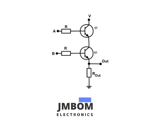
AND Gate based on Transistors
For both transistors, the two inputs connect to the base terminal. These inputs let the current flow through the two transistors. When the input signal is HIGH, current flows through the transistors, and you’ll get the full voltage on the output pin.
Now, if one of the input pins is LOW, the output will also be LOW because the transistors aren’t supplying current. The output won’t vary based on the type of AND gate; it will always follow the truth table for AND gates, which is shown below.
A single AND gate or even a combination of two AND gates can’t be used to create other logic gates. But the AND gate can actually be used to build other types of logic gates!
For example, you can turn an AND gate into a NAND gate just by adding one NOT gate. The AND gate is super important when it comes to designing other logic gates like XNOR and XOR. However, to create these other gates, you’ll also need OR and NOT gates.
Applications of 74LS08
So, here are some applications of the 74LS08 AND Gate IC:
- This IC is mainly used for general-purpose AND gate logic.
- You’ll find it in various devices like servers, ALUs, digital electronics, memory units, and networking devices.
- It's also used in a bunch of digital systems.
- Basically, this IC is perfect whenever you need the logic operation of an AND gate. It has 4 AND gates, so you can use one gate or all of them at the same time.
- This IC is super handy where you need high-speed operation for AND gates.
- The logic gates are built with Schottky transistors, which help reduce switching delays. So, this IC can handle AND operations really quickly.
- Plus, it’s quite affordable for AND gate logic operations and is pretty popular and easy to find.
Frequently Asked Questions
What’s the Difference Between 74HC08 and 74LS08?
So, when we look at the 7400 Series, specifically the 74HC08 and 74LS08 AND gates, one key difference is that the 74HC08 can handle a voltage range of 2V to 6V, while the 74LS08 is only good for 5V. Once you connect either chip, you can use any of the four basic AND gates inside. Just keep in mind that the current you can draw from each AND gate depends on which chip you’re using.
Who Manufactures IC 74LS08?
The 74LS08 is made by Texas Instruments.
Can I Replace 74LS with 74HC?
In many cases, the 74HC can be a better replacement for the 74LS because it offers better power consumption and characteristics. If you’re looking for a closer match to the existing 74LS logic in terms of input threshold, then the 74HCT is the way to go.
What’s the Difference Between HC and LS Chips?
The main difference is in the logic levels. The HC chips need a minimum of 3.5V at 5Vcc for the high logic level, while LS chips only need anything above 2.0V at 5Vcc to be considered logic 1. So, you have to be careful about what you connect to the input of HC logic circuits.
What’s the Use of 74HC08?
The 74HC08 is a Quad 2-Input AND Gate, and it comes in a PDIP-14 package. This design allows you to use current limiting resistors to connect inputs to voltages that exceed VCC. Plus, it’s a pin-compatible replacement for the 74LS08, with better electrical properties and a wider power supply voltage range.
Can the Output of the 74LS Series Logic Gates Drive 74HC Logic Gates?
Just a heads up: 74HC inputs can’t be reliably driven by 74LS outputs because the voltage ranges for logic 0 aren’t fully compatible. So, it’s better to use 74HCT instead.
Final Words
So, that’s a quick overview of the 74LS08 AND Gate IC datasheet. This single IC gives you 4 AND gates, and it’s way cheaper than making one by hand. It’s small, too, and comes in different packages, making it great for fitting into smaller devices. You can use the 74LS08 AND Gate IC with any TTL device without needing extra interface stuff.
Now, here’s a question for you: what are the advantages of the 74LS08 logic gate IC?

Christopher Anderson
Christopher Anderson has a Ph.D. in electrical engineering, focusing on power electronics. He’s been a Senior member of the IEEE Power Electronics Society since 2021. Right now, he works with the KPR Institute of Engineering and Technology in the U.S. He also writes detailed, top-notch articles about power electronics for business-to-business electronics platforms.
Subscribe to JMBom Electronics !


