


FT2232C Dual USB UART/FIFO Interface
Catalog
Key Features SummaryGeneral DescriptionFeatures and EnhancementsSimplified Block DiagramFunctional Block DescriptionsDevice Pin-OutPin DefinitionsOscillator ConfigurationsEEPROM ConfigurationConclusion
Introduction
The FT2232C represents the third generation of FTDI’s well-known USB UART/FIFO IC lineup. It incorporates two versatile UART/FIFO controllers, each configurable for a range of operational modes. Beyond supporting UART, FIFO, and Bit-Bang I/O functions found in the previous FT232BM and FT245BM devices, the FT2232C introduces several advanced interfaces—most notably the Multi-Protocol Synchronous Serial Engine (MPSSE), specifically optimized for synchronous serial communication standards such as JTAG and SPI.
FT2232C
Key Features Summary
Hardware Features
• Integrated USB-to-dual-channel serial/parallel ports with flexible configuration options
• Complete on-chip USB protocol handling—no need for custom USB firmware
• FT232BM-compatible UART interface supporting full handshaking and modem control signals
• UART interface configurable for 7/8-bit data, 1/2 stop bits, and various parity options (Odd, Even, Mark, Space, or None)
• Data transfer rates from 300 bps up to 1 Mbps for RS232, and up to 3 Mbps for TTL and RS422/RS485 levels
• Automatic transmit enable (TXDEN) control for RS485 applications
• FT245BM-compatible FIFO interface featuring bidirectional data bus and simple 4-wire handshake
• Supports data throughput up to 1 MB/s
• Enhanced Bit-Bang mode and new Synchronous Bit-Bang mode for flexible I/O control
• New MPSSE interface designed for synchronous serial protocols like JTAG and SPI
• MCU Host Bus Emulation mode for direct microcontroller interfacing
• Fast Opto-Isolated Serial Interface mode for isolation-based applications
• Configurable USB description strings and interface modes stored in external EEPROM
• On-board EEPROM programmable via USB connection
• USB Suspend/Resume signal support through PWREN# and SI/WU pins
• Compatible with bus-powered, self-powered, and high-power USB configurations
• Built-in Power-On Reset with optional external Reset input/output
• Supports both 5V and 3.3V logic levels with per-channel level conversion
• Integrated 3.3V LDO regulator for USB I/O power
• Built-in PLL clock multiplier (6 MHz–48 MHz)
• Supports both bulk and isochronous USB transfer modes
• Operates from a single 4.35V to 5.25V supply
• Fully compatible with UHCI, OHCI, and EHCI USB host controllers
• Complies with USB 2.0 Full-Speed (12 Mbps) specification
• Compact 48-pin LQFP package
Virtual COM Port (VCP) Drivers Available For:
• Windows 98 / 98 SE / 2000 / ME / XP
• Linux 2.4.0 and later
• Windows CE
• Mac OS 8 / 9**
• Mac OS X
D2XX Direct Driver + DLL Software Interface For:
• Windows 98 / 98 SE / 2000 / ME / XP
• Linux 2.4 and above
Typical Applications
• Dual-port USB to RS232 converters
• Dual-port USB to RS422/RS485 converters
• USB upgrades for legacy serial devices
• USB-based instrumentation systems
• USB JTAG programming tools
• USB-to-SPI bus interfaces
• USB industrial control equipment
• Field-upgradable USB products
• USB-connected opto-isolated systems
General Description
The FT2232C is a USB interface IC that integrates the functionality of two of FTDI’s second-generation BM-series chips into a single package. It converts a single downstream USB port into two independent I/O channels, each configurable as either a FT232BM-style UART interface or a FT245BM-style FIFO interface—eliminating the need for an external USB hub.
Additionally, several new operation modes are available through configuration in the external EEPROM or via driver commands. These include Synchronous Bit-Bang Mode, CPU-Style FIFO Interface Mode, Multi-Protocol Synchronous Serial Engine (MPSSE) Mode, MCU Host Bus Emulation Mode, and Fast Opto-Isolated Serial Interface Mode. A new high-drive output option allows the UART/FIFO I/O pins to deliver approximately three times the standard drive strength, enabling shared bus operation across multiple devices.
The device also supports the traditional BM-style Asynchronous Bit-Bang Mode, now enhanced to provide access to internal RD# and WR# strobes for improved flexibility.
FTDI supplies a royalty-free Virtual COM Port (VCP) driver, making the FT2232C’s ports appear as standard COM ports on a PC. Most existing serial communication software can interface directly by simply selecting the new virtual ports created by the driver. Through the VCP driver, developers can communicate with the FT2232C just as they would with a standard PC COM port using Windows VCOMM API calls or a COM port library.
In addition, the FT2232C driver includes full support for FTDI’s D2XX driver functions, enabling developers to communicate directly with the hardware using a Windows DLL for advanced USB control.
Features and Enhancements
Two Independent I/O Channels
Each channel (A and B) of the FT2232C can be independently configured as a FT232BM-style UART or a FT245BM-style FIFO interface. Both channels also support several special I/O operating modes.
Integrated Power-On-Reset (POR) Circuit
The chip includes a built-in Power-On-Reset circuit. A RESET# pin allows for optional external reset control, though it can typically be tied to VCC. The RSTOUT# pin can be used to deliver a clean, stable reset signal to external microcontrollers or other connected devices.
Integrated RCCLK Circuit
This feature ensures that the oscillator and clock multiplier PLL achieve frequency stability before USB enumeration begins, improving startup reliability.
Built-in Level Conversion
Each channel has a dedicated VCCIO pin (3V–5V range), enabling independent voltage level configuration. This makes it possible to connect 3.3V logic directly without needing external level shifters.
Enhanced Power Management for High-Power USB Devices
The PWREN# pin activates once the device is enumerated by USB and deactivates when entering USB suspend mode. It can drive a transistor or P-channel MOSFET for external power switching. Additionally, the BM-series “pull-down enable” feature is retained—ensuring that, when power is removed, any remaining voltage on I/O lines is safely discharged to ground, allowing reliable reset behavior upon power restoration.
Isochronous USB Transfer Support
While bulk transfer is typically preferred for data throughput, the FT2232C also supports isochronous transfer for applications where timing consistency is critical (e.g., low-bandwidth audio or video transmission). This option can be enabled via EEPROM configuration.
Send Immediate / Wake-Up (SI/WU) Pin on Each Channel
Each channel includes a combined Send Immediate/Wake-Up pin. When USB is suspended (and remote wakeup is enabled in EEPROM), pulling this pin low triggers a USB resume signal, waking the host system. During normal operation, strobing this pin forces immediate transmission of any data in the RX buffer, regardless of packet size—helpful for optimizing latency in time-sensitive applications.
Ultra-Low Suspend Current
The FT2232C consumes less than 100 μA (excluding the 1.5K pull-up resistor on USBDP) in USB suspend mode. This low standby current helps ensure compliance with the USB suspend current limit of 500 μA, leaving more headroom for connected peripheral circuits.
Programmable Receive Buffer Timeout
The FT2232C includes a programmable transmit (TX) buffer timeout feature, adjustable via USB in 1 ms increments from 1 ms to 255 ms. This flexibility allows system designers to fine-tune data handling, optimizing device response time for communication protocols that depend on quick reactions to short data packets.
Improved Power Supply Decoupling
The enhanced VCC decoupling technique first introduced in the BM-series chips has been carried over into the FT2232C design. This improvement ensures greater noise immunity and overall stability of the device under varying load and supply conditions.
Baud Rate Pre-Scaler Divisors
In UART mode, the FT2232C supports fine-grained baud rate control through fractional pre-scaler division. The available divisors include (n + 0), (n + 0.125), (n + 0.25), (n + 0.375), (n + 0.5), (n + 0.625), (n + 0.75), and (n + 0.875), where n is any integer between 2 and 16,384 (2¹⁴). This expanded fractional division capability enables precise baud rate tuning to match specific communication requirements.
Extended EEPROM Compatibility
The FT2232C supports several EEPROM types, including the 93C46 (64 × 16-bit), 93C56 (128 × 16-bit), and 93C66 (256 × 16-bit) devices. While the FT2232C itself does not use all of the additional memory space, it can be accessed by an external MCU or logic circuitry while the FT2232C is held in reset. When a 93C56 or 93C66 EEPROM is used, an additional 64 words (128 bytes total) of user-accessible memory becomes available for custom data storage.
USB 2.0 Full-Speed Option
Through an EEPROM configuration option, the FT2232C can identify itself as a USB 2.0 device instead of USB 1.1. Note that this configuration supports USB 2.0 Full-Speed operation (12 Mb/s) rather than USB 2.0 High-Speed (480 Mb/s). This provides compatibility with modern USB 2.0 systems while maintaining reliable full-speed performance.
FT2232C Dual USB UART / FIFO Interface Chip
Beyond the features of the BM series chips, the FT2232C introduces several enhanced capabilities and interface modes:
Enhanced Asynchronous Bit-Bang Interface
The FT2232C retains compatibility with FTDI’s BM series Bit-Bang mode. In this mode, the eight FIFO data lines can toggle between FIFO operation and functioning as an 8-bit parallel I/O port. Data packets sent to the device are output sequentially at a rate defined by an internal timer (similar to a baud rate prescaler).
With the FT2232C, this feature is upgraded—its internal RD# and WR# strobes are now available externally, allowing connected logic circuits to be synchronized with Bit-Bang bus operations.
Synchronous Bit-Bang Interface
Unlike the asynchronous version, Synchronous Bit-Bang mode reads data only when a write occurs. This makes it easier for the host software to measure responses to output signals, since incoming data is synchronized with outgoing data.
High-Drive Output Capability
The I/O pins can operate at up to three times the standard output drive strength. This enables direct connection to multiple external devices or components that require stronger drive levels. Configuration of this feature is done via the external EEPROM and can be set independently for each channel.
Multi-Protocol Synchronous Serial Engine (MPSSE)
The MPSSE is designed for seamless communication with synchronous serial interfaces such as JTAG or SPI. It offers high flexibility, supporting both industry-standard and custom bus protocols.
For example, one FT2232C channel can be connected to an SRAM-configurable FPGA from suppliers like Altera or Xilinx. At power-up, the FPGA is initially unconfigured. The PC application can then use the MPSSE to download configuration data over USB, defining the FPGA’s hardware function. The second FT2232C channel remains free for other purposes.
This setup enables developers to design a “universal” USB peripheral whose function can be modified by software simply by updating the FPGA configuration file. (See FTDI’s MORPHIC development module at www.morph-ic.com for a practical example.)
MCU Host Bus Emulation
This mode merges the ‘A’ and ‘B’ bus interfaces, allowing the FT2232C to emulate a traditional 8048/8051 microcontroller bus. This makes it possible to directly interface with peripherals designed for these MCU families, enabling USB-based I/O operations with assistance from the MPSSE engine.
Fast Opto-Isolated Serial Interface
A proprietary FTDI protocol enables synchronous communication between the FT2232C and galvanically isolated devices using just four signal lines (via two dual opto-isolators) and two power lines. The peripheral circuit manages bidirectional data rates while maintaining data integrity, achieving full USB speed performance. Both channels ‘A’ and ‘B’ can share the same 4-wire link if required.\
FT2232C Dual USB UART / FIFO I.C.
Simplified Block Diagram
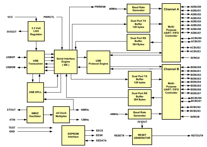
FT2232C Simplified Block Diagram
Functional Block Descriptions
3.3V LDO Regulator
The 3.3V Low Dropout (LDO) Regulator provides a stable 3.3V reference voltage for powering the USB transceiver output buffers. An external decoupling capacitor must be connected to the 3V3OUT pin. It also supplies 3.3V to the RSTOUT# pin.
The main role of this regulator is to power the USB Transceiver and Reset Generator circuits, rather than external components. However, if needed, external circuits that require a nominal 3.3V and draw less than 5mA can source power from the 3V3OUT pin.
USB Transceiver
The USB Transceiver provides the physical layer interface for USB 1.1 and USB 2.0 full-speed communication. Its output drivers generate 3.3V signal levels with controlled slew rates, while a differential receiver and two single-ended receivers handle USB data input, Single-Ended Zero (SEO) detection, and USB reset signal detection.
USB DPLL
The USB Digital Phase-Locked Loop (DPLL) synchronizes with incoming NRZI-encoded USB data and outputs separate recovered clock and data signals to the Serial Interface Engine (SIE).
6MHz Oscillator
This oscillator generates a stable 6MHz reference clock for the x8 Clock Multiplier using an external 6MHz crystal or ceramic resonator.
x8 Clock Multiplier
The x8 Clock Multiplier amplifies the 6MHz oscillator input to 48MHz. This 48MHz reference clock drives both the USB DPLL and the Baud Rate Generator circuits.
Serial Interface Engine (SIE)
The SIE performs the conversion between parallel and serial data streams in compliance with the USB 2.0 specification. It also handles bit stuffing/unstuffing and CRC5/CRC16 generation and verification on the USB data stream.
USB Protocol Engine
The USB Protocol Engine manages data flow through the USB control endpoint. It handles low-level USB protocol requests (Chapter 9 operations) from the USB host controller and interprets commands for configuring the UART/FIFO control blocks.
Dual-Port TX Buffers (128 bytes)
Data received from the USB OUT endpoint is stored in the dual-port TX buffer. The UART/FIFO controller retrieves this data from the buffer for transmission.
Dual-Port RX Buffers (384 bytes)
Incoming data from the UART/FIFO controller’s receive register is temporarily stored in the dual-port RX buffer. The SIE retrieves this data when the USB IN endpoint requests it.
Multi-Purpose UART / FIFO Controllers
These controllers manage data transfer between the dual-port RX/TX buffers and the UART/FIFO registers.
When configured as a UART, the controller performs asynchronous 7-bit or 8-bit parallel-to-serial and serial-to-parallel conversion for RS232, RS422, or RS485 interfaces.
Supported control signals include RTS, CTS, DSR, DTR, DCD, and RI. Transmitter enable pins (TXDEN) are also available for driving RS485 transceivers.
The UART supports RTS/CTS, DSR/DTR, and Xon/Xoff flow control options, all handled in hardware for fast response. It also includes RS232 BREAK detection and generation features.
Baud Rate Generator
This block provides a 16x clock source to the UARTs derived from the 48MHz reference clock. It includes a 14-bit prescaler and three fine-tuning bits to allow fractional division, giving precise control over the baud rate.
The UART baud rate is programmable from 183 baud up to 3 Mbps.
Reset Generator
The Reset Generator provides a stable power-on reset for the device’s internal logic. External RESET# input and RSTOUT# output pins allow the FT2232C to be reset by external logic or to reset other devices.
During reset, RSTOUT# is driven low; otherwise, it outputs 3.3V from the internal regulator. RSTOUT# can directly control the 1.5K pull-up resistor on the USBDP line for delayed USB enumeration or can reset external circuits.
RSTOUT# remains high impedance for approximately 5ms after VCC exceeds 3.5V, the oscillator is running, and RESET# is high. RESET# should be tied to VCC unless external reset control is needed.
FT2232C Dual USB UART / FIFO Interface Chip
EEPROM Interface
When operated without an external EEPROM, the FT2232C automatically configures itself as a USB-to-dual-serial-port device.
By adding an external 93C46, 93C56, or 93C66 EEPROM, each of the FT2232C’s two channels can be independently configured as either a serial UART (232 mode) or a parallel FIFO (245 mode).
The external EEPROM also enables additional features, including the Fast Opto-Isolated Serial Interface mode. Furthermore, it allows customization of various USB parameters such as:
- Vendor ID (VID) and Product ID (PID)
- Device Serial Number
- Product Description Strings
- Power Descriptor value
This makes it ideal for OEM applications requiring unique identification or branding.
Other configuration options stored in the EEPROM include Remote Wake-Up capability, Isochronous Transfer Mode, Soft Pull-Down on Power-Off, and USB 2.0 descriptor settings.
The EEPROM should be a 16-bit-wide device, such as the Microchip 93LC46B or an equivalent part, capable of operating at a 1 Mb/s clock rate when VCC is between 4.35 V and 5.25 V.
It can be programmed directly over USB using FTDI’s utility software, available from www.ftdichip.com. This allows blank EEPROMs to be mounted on the PCB and programmed during the manufacturing or testing process.
If no EEPROM is connected—or if a blank EEPROM is installed—the FT2232C defaults to a dual serial port configuration. In this state, the device uses its built-in default VID, PID, product description, and power descriptor values, and it does not include a serial number in its USB descriptor.
Device Pin-Out
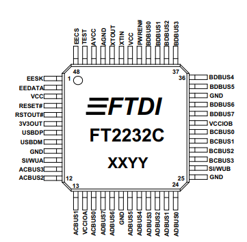
Pin-Out(LQFP-48 Package )
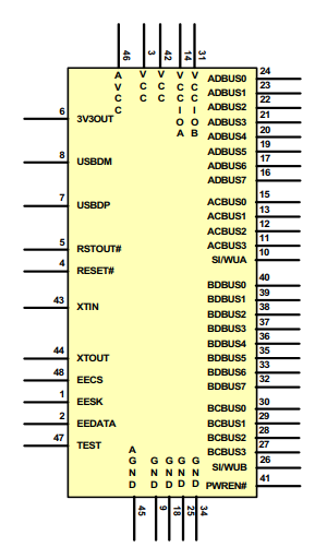
(Schematic Symbol )
Pin Definitions
This section describes the function of each pin on the FT2232C.
Common pins are listed first, followed by I/O pins, which vary depending on the chip mode.
More detailed explanations of I/O pin behavior are provided in Section 9.
5.1 Common Pins
The pins described below operate the same way in all FT2232C modes.
USB Interface Group
| Pin # | Signal | Type | Description |
|---|---|---|---|
| 7 | USBDP | I/O | USB Data Signal Plus. Requires a 1.5kΩ pull-up resistor to 3V3OUT or RSTOUT#. |
| 8 | USBDM | I/O | USB Data Signal Minus. |
EEPROM Interface Group
| Pin # | Signal | Type | Description |
|---|---|---|---|
| 48 | EECS | I/O | EEPROM Chip Select. Tri-stated during device reset. Note 1 |
| 1 | EESK | OUTPUT | Clock signal for the EEPROM. Tri-stated during reset; otherwise drives normally. Note 1 |
| 2 | EEDATA | I/O | EEPROM Data I/O. Connect directly to the EEPROM’s Data-In pin and to its Data-Out pin through a 2.2kΩ resistor. The EEPROM’s Data-Out pin must also be pulled up to VCC using a 10kΩ resistor to ensure correct operation. Tri-stated during reset. Note 1 |
Miscellaneous Signal Group
| Pin # | Signal | Type | Description |
|---|---|---|---|
| 4 | RESET# | INPUT | External reset input for the FT2232C. Tie to VCC if not used. Note 1 |
| 5 | RSTOUT# | OUTPUT | Output from the internal Reset Generator. Driven low for approximately 5.6 ms after VCC exceeds 3.5V and the internal clock starts, then outputs 3.3V from the internal regulator. Pulling RESET# low forces RSTOUT# low as well. This signal is not affected by a USB bus reset. |
| 47 | TEST | INPUT | Enables the device’s internal test mode. Must be tied to GND during normal operation. |
| 41 | PWREN# | OUTPUT | Goes low once the device has been configured via USB and returns high during USB suspend. Can be used to control external power circuitry using a P-channel logic-level MOSFET switch. When using PWREN#, enable the Interface Pull-Down Option in the EEPROM. |
| 43 | XTIN | INPUT | Input to the 6MHz crystal oscillator cell. Can also accept an external 6MHz clock. Note: The switching threshold is VCC/2, so an external clock must either operate at 5V CMOS levels or be AC-coupled to center around VCC/2. |
| 44 | XTOUT | OUTPUT | Output from the 6MHz crystal oscillator cell. Oscillation stops during USB suspend mode, so avoid using this output to clock external logic directly. |
Power and Ground Group
| Pin # | Signal | Type | Description |
|---|---|---|---|
| 6 | 3V3OUT | OUTPUT | 3.3V output from the integrated LDO regulator. This pin should be decoupled to ground with a 33nF ceramic capacitor placed close to the pin. Its primary function is to supply 3.3V power to the USB transceiver and RSTOUT# circuits. A small current (up to 5mA) can also be drawn from this pin to power external 3.3V logic if needed. |
| 3, 42 | VCC | PWR | +4.35V to +5.25V supply voltage for the device core, LDO regulator, and non-UART/FIFO controller interface pins. |
| 14 | VCCIOA | PWR | +3.0V to +5.25V supply for the Channel A UART/FIFO interface pins (pins 10–13, 15–17, and 19–24). When connecting to 3.3V logic in a bus-powered design, tie VCCIOA to a 3.3V source derived from the USB bus. For self-powered designs using 3.3V logic, connect VCCIOA to the external 3.3V supply. Otherwise, connect to VCC for 5V CMOS-level operation. |
| 31 | VCCIOB | PWR | +3.0V to +5.25V supply for the Channel B UART/FIFO interface pins (pins 26–30, 32–33, and 35–40). When interfacing with 3.3V logic in a bus-powered system, connect VCCIOB to a 3.3V source generated from the USB bus. In a self-powered system, tie VCCIOB to the external 3.3V supply. Otherwise, connect to VCC for 5V CMOS-level output. |
| 9, 18, 25, 34 | GND | PWR | Ground supply pins for the device. |
| 46 | AVCC | PWR | Analog power supply for the internal x8 clock multiplier. A low-pass filter consisting of a 470Ω series resistor and a 100nF capacitor to ground should be used on this pin. |
| 45 | AGND | PWR | Analog ground connection for the internal x8 clock multiplier. |
I/O Mode Command Hex Values
The FT2232C supports several I/O modes that can be enabled via the D2XX driver using the FT_SetBitMode command. The corresponding hexadecimal values for each mode are listed below:
| Mode | Hex Value |
|---|---|
| Reset I/O Bit Mode | 0x00 |
| Asynchronous Bit-Bang Mode | 0x01 |
| Multi-Protocol Synchronous Serial Engine (MPSSE) | 0x02 |
| Synchronous Bit-Bang Mode | 0x04 |
| MCU Host Bus Emulation | 0x08 |
| Fast Opto-Isolated Serial Mode | 0x10 |
For detailed usage examples, see Application Note AN2232C-02: “Bit Mode Functions for the FT2232C.”
Notes:
- All other device modes can be configured via the external EEPROM and do not require FT_SetBitMode.
- For Fast Opto-Isolated Serial Mode, sending 0x10 will hold the mode in reset, while sending 0x00 will release it from reset.
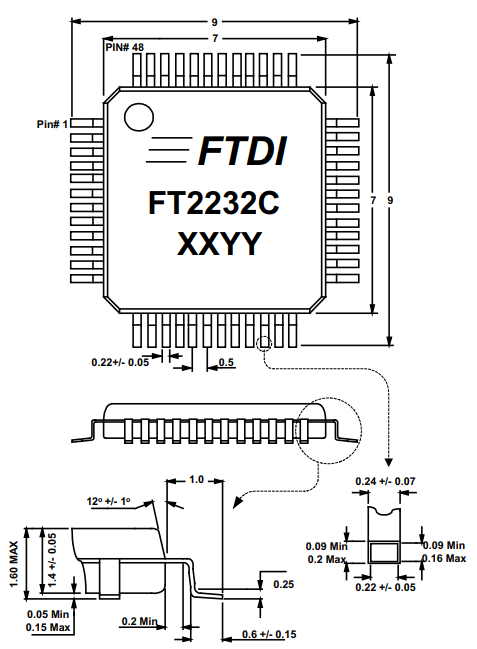
Package Outline
The FT2232C is supplied in a 48 LD LQFP package as standard. This package has a 7mm x 7mm body (9mm x 9mm
including leads) with leads on a 0.5mm pitch.
The above drawing shows the LQFP-48 package – all dimensions are in millimetres.
A Lead free version of this package is also available, part number FT2232L.
XXYY = Date Code ( XX = 2 digit week number, YY = 1 or 2 digit year number.
Figure 4 - 48 LD LQFP Package Dimensions
Oscillator Configurations
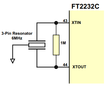
Figure 5 3-Pin Ceramic Resonator Configuration
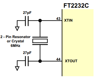
Figure 6 Crystal or 2-Pin Ceramic Resonator
Configuration
Using the FT2232C with Crystals or Ceramic Resonators
3-Pin Ceramic Resonator
Figure 5 shows how to connect the FT2232C to a 3-pin ceramic resonator. A suitable option is a Murata CERALOCK resonator (e.g., Murata Part Number CSTCR6M00G15) or an equivalent part.
3-pin ceramic resonators include internal load capacitors, so no external capacitors are needed, making this a cost-effective configuration. The Murata CSTCR6M00G15 provides an accuracy of ±0.25% and is specifically designed for USB full-speed applications. To ensure this level of accuracy, a 1MΩ resistor should be placed across XTIN and XTOUT.
Resonators with slightly lower accuracy (typically ±0.5%) fall outside strict USB specifications, but calculations show they can still work reliably in FT2232C designs. An example is Murata CSTLSM00G53.
6MHz Crystal or 2-Pin Ceramic Resonator
Figure 6 illustrates using the FT2232C with a 6MHz crystal or a 2-pin ceramic resonator. Unlike 3-pin resonators, these devices do not have built-in load capacitors, so external capacitors must be added between XTIN, XTOUT, and GND.
- A value of 27pF is commonly used and works for many crystals and some resonators.
- Always select the capacitor value based on the manufacturer’s recommendations.
- For crystals, use parallel-cut types.
- For resonators, refer to the earlier note on frequency accuracy.
Using a 6MHz Oscillator
A 6MHz oscillator can also be used with the FT2232C. In this case:
- Connect the oscillator output directly to XTIN.
- Leave XTOUT unconnected.
- Ensure the oscillator provides a CMOS output.
EEPROM Configuration
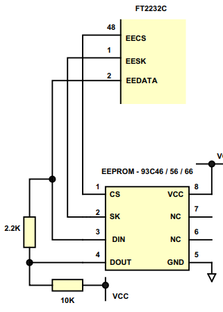
Figure 7 EEPROM Configuration
Connecting the FT2232C to a 93C46 / 93C56 / 93C66 EEPROM
Figure 7 shows how to connect the FT2232C to a compatible EEPROM.
- Pin connections: EECS (Pin 48) → directly to the EEPROM’s Chip Select (CS) pin. EESK (Pin 1) → directly to the EEPROM’s Clock (SK) pin. EEDATA (Pin 2) → directly to the EEPROM’s Data-In (Din) pin.
To prevent potential data conflicts where both the EEPROM’s Data-Out (Dout) and the FT2232C’s EEDATA pin could drive the line simultaneously, the EEPROM’s Dout is connected to EEDATA through a 2.2kΩ resistor.
EEPROM Initialization and Operation:
After a power-on reset or USB reset, the FT2232C performs the following checks:
- Detects whether an EEPROM is present.
- Verifies whether the data in the EEPROM is valid.
- If both checks pass, the FT2232C uses the EEPROM data.
- Otherwise, the device defaults to built-in values, with both Channel A and Channel B configured as serial UARTs.
When the FT2232C sends a valid command to the EEPROM, the EEPROM acknowledges by pulling its Dout pin low. To detect this condition, Dout should be pulled high with a 10kΩ resistor. If no acknowledgment occurs, EEDATA is pulled high by the 10kΩ resistor, signaling either an invalid command or that no EEPROM is present.
EEPROM Requirements:
- The FT2232C requires a 16-bit-wide EEPROM, such as the Microchip 93LC46B.
- The EEPROM must support a 1Mb/s clock rate at a supply voltage of 4.35V–5.25V.
- Check the manufacturer’s datasheet carefully, as pin 6 and 7 configurations vary: some parts use them as NC, others for 8/16-bit selection or test functions. Some EEPROMs have rotated pinouts, so select the correct part and options.
Sharing the EEPROM with Another Device:
It is possible to share the EEPROM between the FT2232C and an external MCU. This can only be done while the FT2232C is in reset, as it tri-states its EEPROM interface during this time.
A typical shared configuration:
- One MCU I/O pin holds the FT2232C in reset (via RESET#) during power-up.
- Three MCU pins connect to EECS, EESK, and EEDATA to read/write EEPROM data.
- Once the MCU finishes accessing the EEPROM, RESET# is released, allowing the FT2232C to configure itself and enumerate over USB.
EEPROM Programming:
- The external EEPROM can be programmed over USB using FTDI’s utility software.
- It is used to enable 245 FIFO mode and Fast Opto-Isolated Serial Interface mode for each channel.
Conclusion
The FT2232C is a versatile dual USB UART/FIFO interface chip that offers multiple configurable I/O modes, including asynchronous and synchronous Bit-Bang, MPSSE, MCU Host Bus Emulation, and Fast Opto-Isolated Serial modes. Its internal blocks—such as the USB transceiver, DPLL, SIE, UART/FIFO controllers, and reset/clock circuits—ensure reliable USB communication and flexible data handling. Power and ground pins, along with configurable VCCIO supplies, support both 3.3V and 5V logic interfacing. External components like crystals, ceramic resonators, and EEPROMs allow precise clocking, mode selection, and device customization, making the FT2232C suitable for a wide range of USB peripheral applications.

Christopher Anderson
Christopher Anderson has a Ph.D. in electrical engineering, focusing on power electronics. He’s been a Senior member of the IEEE Power Electronics Society since 2021. Right now, he works with the KPR Institute of Engineering and Technology in the U.S. He also writes detailed, top-notch articles about power electronics for business-to-business electronics platforms.
Subscribe to JMBom Electronics !


