


MC145012 CMOS Smoke Detector IC – Features, Pin Functions, and Calibration
Catalog
Key Features:PIN ASSIGNMENTBLOCK DIAGRAMElectrical CharacteristicsPIN DESCRIPTIONSCALIBRATIONConclusionThe CMOS MC145012 is a highly advanced smoke detector IC that integrates ultra–low–power analog and digital circuitry. Designed for use with an infrared photoelectric chamber, the device detects smoke by sensing scattered light from fine smoke particles or other aerosols. Once smoke is detected, the IC activates a pulsating alarm through built-in push–pull drivers and an external piezoelectric transducer.
MC145012 CMOS
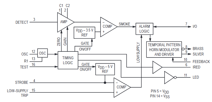
The variable-gain photo amplifier is optimized for direct connection to IR detectors (photodiodes). Two external capacitors, C1 (larger) and C2, set the amplifier gain. The IC automatically adjusts gain depending on the operating mode:
- Low gain during standby,
- Medium gain when smoke is locally detected,
- High gain during the pushbutton test and in periodic chamber sensitivity checks.
For multi-unit systems, the I/O pin with VSS enables interconnection of up to 40 devices for common signaling. An on-chip current sink enhances noise immunity when I/O is configured as input. During a local-smoke event, the short-circuit-protected I/O driver alerts interconnected units. The I/O can also control escape lighting, auxiliary alarms, remote alarms, or auto-dialers.
The IC includes low-supply monitoring, periodically tested with pulsed load current via the LED pin. The trip point is configured with two external resistors, and the system is powered by a standard 9 V battery.
The alarm indicators are intuitive:
- LED flash + pulsing alarm = local smoke detected.
- Pulsing alarm only (no LED) = remote smoke detected.
- Chirp/beep + LED flash = low battery condition.
- Chirp/beep between LED flashes = reduced chamber sensitivity.
Importantly, the IC continues to detect smoke even when the supply voltage drops, as long as VDD ≥ 6 V. To distinguish between low-supply and degraded sensitivity, a pushbutton test can be performed.
Key Features:
- Designed for smoke detection systems compliant with UL217 and UL268 standards
- Operating Voltage: 6 to 12 V
- Operating Temperature: –10°C to +60°C
- Average Supply Current: 8 μA
- Power-On Reset ensures standby (non-alarm) mode at startup
- I/O pin supports up to 40 interconnected units
- Robust ESD and latch-up protection on all pins
- Chip complexity: ~2000 FETs, 12 NPNs, 16 resistors, and 10 capacitors
- Compatible with NFPA 72, ANSI S3.41, and ISO 8201 audible evacuation signal standards
- Optimized for battery-powered applications
PIN ASSIGNMENT
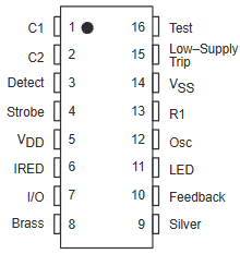
PIN ASSIGNMENT
BLOCK DIAGRAM
BLOCK DIAGRAM
Maximum Ratings
(All voltages referenced to VSS)
| Symbol | Parameter | Value | Unit |
|---|---|---|---|
| VDD | DC Supply Voltage | –0.5 to +12 | V |
| Vin | DC Input Voltage | V | |
| – C1, C2, Detect | –0.25 to VDD +0.25 | ||
| – Osc, Low-Supply Trip | –0.25 to VDD +0.25 | ||
| – I/O | –0.25 to VDD +10 | ||
| – Feedback | –15 to +25 | ||
| – Test | –1.0 to VDD +0.25 | ||
| Iin | DC Input Current per Pin | ±10 | mA |
| Iout | DC Output Current per Pin | ±25 | mA |
| IDD | DC Supply Current (VDD & VSS pins) | +25 / –150 | mA |
| PD | Power Dissipation in Still Air | mW | |
| – for 5 seconds | 1200** | ||
| – continuous | 350*** | ||
| Tstg | Storage Temperature Range | –55 to +125 | °C |
| TL | Lead Temperature (1 mm from case, 10 sec) | 260 | °C |
* Note: Maximum Ratings are limits beyond which permanent device damage may occur. Functional operation should be confined to the ranges specified in the Electrical Characteristics tables.
** Derating: –12 mW/°C from +25°C to +60°C.
*** Derating: –3.5 mW/°C from +25°C to +60°C.
This device includes protection circuitry to reduce risks from static voltage or electric fields. However, exposure to voltages above the specified limits may still damage the high-impedance inputs.
- For reliable operation, keep Vin and Vout within: VSS ≤ (Vin, Vout) ≤ VDD, except: – The I/O pin may exceed VDD, – The Test input may go below VSS.
- Unused inputs must be tied to a valid logic level (VSS or VDD).
- Unused outputs or I/O pins should be left unconnected.
Electrical Characteristics
(All voltages referenced to VSS; TA = –10°C to +60°C unless otherwise noted)
| Symbol | Parameter | Test Condition | VDD (V) | Min | Max | Unit |
|---|---|---|---|---|---|---|
| VDD | Power Supply Voltage Range | — | — | 6 | 12 | V |
| VTH | Low-Supply Alarm Threshold Voltage | Low-supply trip, Vin = VDD/3 | — | 6.5 | 7.8 | V |
| IDD | Average Operating Supply Current (per package, excluding D3–IR emitter current) | Standby, configured per Fig. 5 | 12.0 | — | 8.0 | μA |
| iDD | Peak Supply Current (per package, excluding IRED current into Q1) | Strobe On, IRED Off, per Fig. 5 | 12.0 | — | 2.0 | mA |
| Strobe On, IRED On, per Fig. 5 | 12.0 | — | 3.0 | mA | ||
| VIL | Low-Level Input Voltage | I/O | 9.0 | — | 1.5 | V |
| Feedback | 9.0 | — | 2.7 | V | ||
| Test | 9.0 | — | 7.0 | V | ||
| VIH | High-Level Input Voltage | I/O | 9.0 | 3.2 | — | V |
| Feedback | 9.0 | 6.3 | — | V | ||
| Test | 9.0 | 8.5 | — | V | ||
| Iin | Input Current | OSC, Detect, Low-Supply Trip, Feedback (Vin = VSS or VDD) | 12.0 | — | ±100 | nA |
| IIL | Low-Level Input Current | Test, Vin = VSS | 12.0 | –100 | –1 | μA |
| IIH | Pull-Down Current | Test, Vin = VDD | 9.0 | 0.5 | 10 | μA |
| I/O, no local smoke, Vin = VDD | 9.0 | 25 | 100 | μA | ||
| I/O, no local smoke, Vin = 17 V | 12.0 | — | 140 | μA | ||
| VOL | Low-Level Output Voltage | LED, Iout = 10 mA | 6.5 | — | 0.6 | V |
| LED, Iout = 16 mA | 6.5 | — | 1.0 | V | ||
| VOH | High-Level Output Voltage | LED, Iout = –16 mA | 6.5 | 5.5 | — | V |
| Vout | Strobe Output Voltage | Inactive, Iout = 1 μA | — | VDD – 0.1 | — | V |
| Active, Iout = 100–500 μA (Load Regulation) | 9.0 | VDD – 4.4 | VDD – 5.6 | V | ||
| IRED | Infrared LED Drive Voltage | Inactive, Iout = 1 μA | — | — | 2.25* | V |
| Active, Iout = 6 mA (Load Regulation) | 9.0 | 0.1 | 3.75* | V | ||
| IOH | High-Level Output Current (I/O) | Local smoke, Vout = 4.5 V | 6.5 | –4 | — | mA |
| Local smoke, Vout = VSS (short-circuit current) | 12.0 | — | –16 | mA | ||
| IOZ | Off-State Output Leakage Current | LED, Vout = VSS or VDD | 12.0 | — | ±1 | μA |
| VIC | Common-Mode Input Voltage Range | C1, C2, Detect (local smoke, pushbutton test, chamber sensitivity test) | — | VDD – 4 | VDD – 2 | V |
| Vref | Smoke Comparator Internal Reference Voltage | Local smoke, pushbutton test, chamber sensitivity test | — | VDD – 3.08 | VDD – 3.92 | V |
* TA = 25°C only
AC Electrical Characteristics
(Reference timing diagram: Figures 3 and 4. TA = 25°C, VDD = 9.0 V. Component values from Fig. 5: R1 = 100 kΩ, C3 = 1500 pF, R2 = 7.5 MΩ)
| No. | Symbol | Parameter | Test Condition | Clocks | Min* | Typ** | Max* | Unit |
|---|---|---|---|---|---|---|---|---|
| 1 | 1/fosc | Oscillator Period | Free-running sawtooth, measured at Pin 12 | 1 | 7.0 | 7.9 | 8.6 | ms |
| 2 | tLED | LED Pulse Period | No local smoke, no remote smoke | 4096 | 28.8 | 32.4 | 35.2 | s |
| 3 | Remote smoke, no local smoke | — | Extinguished | — | — | — | ||
| 4 | Local smoke | 64 | 0.45 | 0.5 | 0.55 | s | ||
| 5 | Pushbutton test | 64 | 0.45 | 0.5 | 0.55 | s | ||
| 6 | tw(LED), tw(stb) | LED Pulse Width / Strobe Pulse Width | — | 1 | 7.0 | — | 8.6 | ms |
| 7 | tIRED | IRED Pulse Period | Smoke test | 1024 | 7.2 | 8.1 | 8.8 | s |
| 8 | Chamber sensitivity test (no local smoke) | 4096 | 28.8 | 32.4 | 35.2 | s | ||
| 9 | Pushbutton test | 128 | 0.9 | 1.0 | 1.1 | s | ||
| 10 | tw(IRED) | IRED Pulse Width | Tf* | — | 94 | 116 | μs | |
| 11 | tr | IRED Rise Time | — | — | — | 30 | μs | |
| 12 | tf | IRED Fall Time | — | — | — | 200 | μs | |
| 13 | ton | Temporal Modulation Pulse Width (Silver/Brass) | — | 64 | 0.45 | 0.5 | 0.55 | s |
| 14 | toff | Modulation Off Pulse Width | — | — | 0.45 | 0.5 | 0.55 | s |
| 15 | toffd | Off Duration | — | 192 | 1.35 | 1.52 | 1.65 | s |
| 16 | tCH | Chirp Pulse Period (Silver/Brass) | Low supply or degraded sensitivity | 4096 | 28.8 | 32.4 | 35.2 | s |
| 17 | twCH | Chirp Pulse Width (Silver/Brass) | — | 1 | 7.0 | 7.9 | 8.6 | ms |
| 18 | tRR | Alarm Response Time (I/O Rising Edge to Smoke Alarm) | Remote smoke, no local smoke | — | — | 2! | — | s |
| 19 | tstb | Strobe Out Pulse Period | Smoke test | 1024 | 7.2 | 8.1 | 8.8 | s |
| 20 | Chamber sensitivity test, no local smoke | 4096 | 28.8 | 32.4 | 35.2 | s | ||
| 21 | Low supply test, no local smoke | 4096 | 28.8 | 32.4 | 35.2 | s | ||
| 22 | Pushbutton test | — | — | 1 | — | s |
Oscillator period T (Tr + Tf) depends on external components R1, R2, and C3, where:
- Tr = 0.6931 × R2 × C3
- Tf = 0.6931 × R1 × C3
Typical values are for reference only and not guaranteed.
! Response time depends on the point within the oscillator cycle where the input signal is applied.
Note: Timing parameters are designed to meet the requirements of NFPA 72, ANSI S3.41, and ISO 8201 audible emergency evacuation signal standards.
MC145012
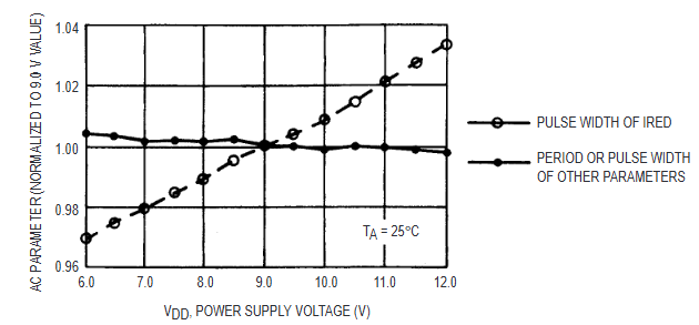
AC Characteristics versus Supply
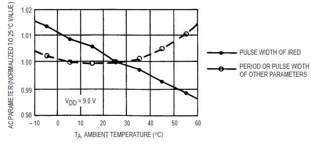
A. AC Characteristics versus Temperature
NOTE: Includes external component variations. See Figure 2B
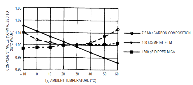
B. RC Component Variation Over Temperature
NOTE: These components were used to generate Figure 2A
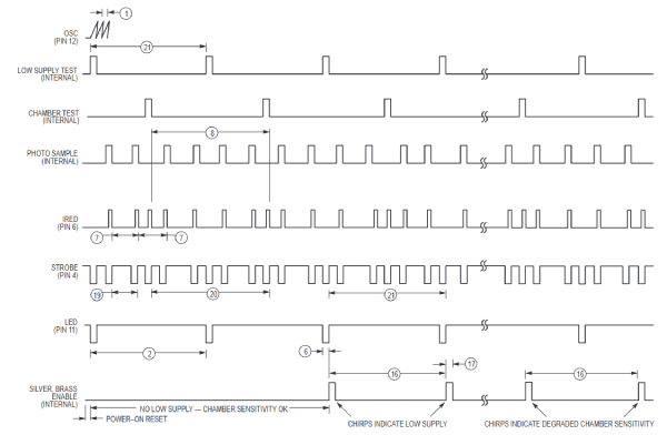
Typical Standby Timing
NOTES: Numbers refer to the AC Electrical Characteristics Table.
Illustration is not to scale.
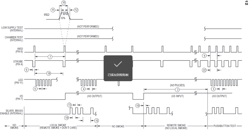
Typical Local Smoke Timing
NOTES: Numbers refer to the AC Electrical Characteristics Table.
Illustration is not to scale.
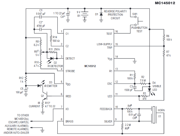
Typical Battery–Powered Application
The values of R4, R5, and C6 may vary depending on the type of piezoelectric horn selected.
C2 and R13 provide coarse sensitivity adjustment. Typical values are shown.
R9 allows fine sensitivity adjustment (optional). If fixed resistors are used instead: – Set R8 = 12 kΩ – Use R10 = 5.6 kΩ to 10 kΩ – Eliminate R9
When R9 is included, the circuit becomes more prone to noise pickup due to antenna effects, and shielding may be required.
C4 should be 22 μF if using a carbon battery. For an alkaline battery, C4 can be reduced to 1 μF.
PIN DESCRIPTIONS
C1 (Pin 1)
A capacitor connected here (see Figure 5) sets the gain of the on-chip photo amplifier during the pushbutton test and chamber sensitivity test (high gain mode).
- The capacitor value must be selected so that, during the pushbutton test, the alarm trips due to background reflections in the chamber.
- Av≈1+C110A_v ≈ 1 + \frac{C1}{10}Av≈1+10C1
- Caution: The closed-loop gain must not exceed 10,000.
C2 (Pin 2)
A capacitor connected here (see Figure 5) sets the gain of the photo amplifier during normal operation (i.e., except during pushbutton or chamber sensitivity tests).
- Av≈1+C210A_v ≈ 1 + \frac{C2}{10}Av≈1+10C2
- This gain increases by about 10% during the IRED pulse after two consecutive local smoke detections.
- R14≈112C2−680R14 ≈ \frac{1}{12\sqrt{C2}} - 680R14≈12C21−680
DETECT (Pin 3)
This pin connects to the cathode of an external photodiode and serves as the input to the high-gain pulse amplifier.
- The photodiode must have low capacitance and low dark leakage current.
- It should be shunted by a load resistor and operated at zero bias.
- The Detect input must be properly ac/dc decoupled from all other signals, VDD, and VSS.
- Keep lead lengths and PCB traces to this pin as short as possible (see Figure 6).
STROBE (Pin 4)
This output provides a strobed, regulated voltage referenced to VDD.
- Temperature coefficient: ±0.2%/°C (max) from –10 °C to +60 °C
- Line regulation: ±0.2%/V (max) from 6 V to 12 V supply
- The strobe output is connected to the external resistor string R8, R9, and R10.
PIN DESCRIPTIONS (continued)
VDD (Pin 5)
- Connects to the positive supply potential, which may range from +6 V to +12 V relative to VSS.
- Caution: In battery-powered designs, external reverse-polarity protection must be included.
IRED (Pin 6)
- Provides pulsed base current to an external NPN transistor (Q1) that drives the infrared emitter.
- Requirements for Q1: β ≥ 100.
- At 10 mA, the output voltage has a typical temperature coefficient of +0.5%/°C (–10 °C to +60 °C).
- Line regulation: ±0.2%/V (max) over 6–12 V supply range.
- Pulse width (active-high) is set by R1 and C3. With R1 = 100 kΩ and C3 = 1500 pF, nominal width ≈ 105 μs.
- Noise immunity: IRED is inactive while the visible LED and horn outputs are active.
- During smoke tests, chamber sensitivity tests, and pushbutton tests, IRED pulses occur near the end of strobe cycles.
I/O (Pin 7)
- Supports interconnection of up to 40 units in a wired-OR configuration using VSS as return.
- An on-chip current sink reduces noise pickup in standby and eliminates the need for an external pull-down resistor.
- Remote units at lower VDD do not draw excessive current from higher-VDD units.
- Can also control escape lights, auxiliary alarms, remote alarms, or auto-dialers.
- As an input, it feeds a positive-edge-triggered flip-flop sampled once per second during standby (with recommended component values).
- In local smoke or pushbutton test mode, the I/O pin sources current, forcing remote signaling.
- All input signals are ignored while sourcing.
- I/O is disabled at power-on reset to prevent false alarms during battery replacement or startup.
- If unused, leave unconnected.
BRASS (Pin 8)
- One half of the push–pull horn driver output.
- Connects to the metal electrode of the piezoelectric transducer and the horn-starting resistor.
- Produces a continuous modulated tone during a smoke alarm (local or remote).
- Produces a short beep/chirp for trouble alarms (low supply or reduced chamber sensitivity).
SILVER (Pin 9)
- The other half of the push–pull horn driver output.
- Connects to the ceramic electrode of the piezoelectric transducer and the horn-starting capacitor.
FEEDBACK (Pin 10)
- Input connected to the feedback electrode of a self-resonating piezoelectric transducer.
- Also connected to the horn-starting resistor and capacitor through R4 (current-limiting).
- If unused, tie this pin to VSS or VDD.
LED (Pin 11)
- Active-low open-drain output that drives an external visible LED.
- Pulse width equals the oscillator period.
- Also applies load during low-supply test (not coincident with smoke or test alarms).
- Visual status indications (typical values with Figure 5 components): Standby (including low-supply and chamber tests): pulse every 32.4 s Local smoke: pulse every 0.51 s Remote smoke: no pulses Pushbutton test: pulse every 0.51 s
OSC (Pin 12)
- Works with R2 (7.5 MΩ to VDD) and C3 (1500 pF to VDD) to form an oscillator.
- Nominal oscillator period ≈ 7.9 ms.
R1 (Pin 13)
- Works with R1 (100 kΩ, to Pin 12) and C3 (1500 pF, see Pin 12) to set the IRED pulse width.
- With this RC network, nominal pulse width ≈ 105 μs.
VSS (Pin 14)
- Negative supply potential.
- Provides the return for both the circuit and the I/O pin.
- Typically tied to ground.
LOW-SUPPLY TRIP (Pin 15)
- Connects to an external voltage divider that sets the low-supply alarm threshold.
- Vtrip≈5R7R6+5V_{trip} ≈ \frac{5R7}{R6} + 5Vtrip≈R65R7+5
TEST (Pin 16)
- Input with an on-chip pull-down device. Used to manually activate the pushbutton test mode.
- Applying a logic high (via a normally-open pushbutton to VDD) initiates test mode after one oscillator cycle: IRED pulses at ~1 s intervals regardless of smoke. Amplifier gain increases by automatic selection of C1, so background reflections mimic smoke. After the second IRED pulse, the horn driver and I/O outputs activate, simulating a smoke alarm. Releasing the button returns the input to VSS via the pull-down.
- After one oscillator cycle, gain returns to normal and the simulated-smoke condition is cleared.
- Within two additional IRED pulses (<3 s), the IC exits alarm mode and returns to standby.
CALIBRATION
The MC145012 includes a calibration mode to simplify detector sensitivity verification and adjustment. In this mode, certain device pins are internally reconfigured (see Table 1 for details).
- Entering Calibration Mode: Pull the Test pin (Pin 16) below VSS. Continuously draw 100 μA from the Test pin for at least one complete OSC cycle.
- Exiting Calibration Mode: Allow the Test pin to float (no current drawn) for at least one OSC cycle.
- Operation in Calibration Mode: The IRED pulse rate is increased to one pulse per OSC cycle, accelerating the test process. The Strobe output remains active low continuously during this mode.
Table 1. Configuration of Pins in Calibration Mode
| Pin | Name | Description / Function in Calibration Mode |
|---|---|---|
| 7 | I/O | Disabled as an output. Forcing this pin high places the photo amplifier output on Pin 1 (C1) or Pin 2 (C2), depending on the state of Low–Supply Trip (Pin 15). Output appears as pulses referenced to VDD. |
| 15 | Low–Supply Trip | When I/O (Pin 7) is high: – Low: Normal gain, amplifier output on Pin 1 (C1). – High: Supervisory gain, amplifier output on Pin 2 (C2). |
| 10 | Feedback | Driving this input high enables hysteresis (≈ 10% gain increase) in the photo amplifier. Pin 15 must be low for hysteresis to apply. |
| 12 | OSC | Driving this pin high holds the internal clock high; driving it low holds the internal clock low. If the RC oscillator network is left intact, the oscillator runs similarly to normal operation. |
| 9 | Silver | Reconfigured as the smoke comparator output. When OSC is toggling, positive pulses indicate smoke detection; a static low level indicates no smoke. |
| 8 | Brass | Reconfigured as the smoke integrator output. Two consecutive smoke detections generate a static high (“on”); two consecutive no-detections generate a static low (“off”). |
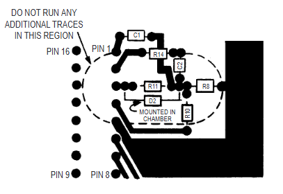
Recommended PCB Layout
NOTES
- Illustration shows bottom view for DIP layout. For SOIC layout, use the mirror image (top view).
- Optional potentiometer R9 is not included in the illustration.
- Drawing is not to scale.
- Leads and traces connected to D2, R11, R8, and R10 must be kept as short as possible to minimize noise pickup.
- Pin 3 (Detect input) must be decoupled from all other traces for reliable operation.
Conclusion
The MC145012 CMOS Smoke Detector IC is a highly integrated, low-power device designed for reliable smoke detection and alarm signaling. It features precise analog and digital circuitry, adjustable photo amplifier gain, and versatile I/O for interconnecting multiple units or controlling external devices. The IC supports comprehensive test and calibration modes, including pushbutton and chamber sensitivity tests, while providing visual (LED) and audible (piezoelectric horn) indicators. Careful design considerations—such as pin decoupling, short trace routing, and optional component adjustments—ensure accurate detection, low noise, and compatibility with battery-powered applications. Overall, the MC145012 offers a complete, flexible solution for smoke detection systems compliant with UL, NFPA, and ISO standards.

Amanda Miller
Amanda Miller is a senior electronics engineer with 6 years of experience. She focuses on studying resistors, transistors, and package design in detail. Her deep knowledge helps her bring innovation and high standards to the electronics industry.
Subscribe to JMBom Electronics !


