


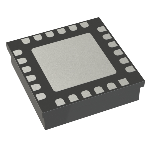
HMC732LC4B Wideband MMIC VCO Overview
Catalog
OverviewKey FeaturesTypical ApplicationsElectrical SpecificationsWIDEBAND MMIC VCO WITH BUFFER AMPLIFIEROutline DrawingPackage InformationEvaluation PCBConclusionOverview
The HMC732LC4B is a wideband MMIC Voltage-Controlled Oscillator (VCO) that integrates the resonator, negative resistance device, and varactor diode into a single compact design. Thanks to its monolithic construction, the oscillator delivers consistent output power and excellent phase noise performance across varying temperatures.
The tuning port supports an analog control voltage from 0 to +23V. Operating from a single +5V supply, the HMC732LC4B draws only 57 mA and comes in a RoHS-compliant surface-mount package. This VCO combines wide tuning range, low power consumption, compact size, and outstanding phase noise in one solution.
Key Features
- Wide tuning bandwidth
- Output power: +1 dBm
- Low SSB phase noise: –95 dBc/Hz @ 100 kHz
- No external resonator required
- Operates from a single +5V supply at 57 mA
- Compact 24-lead 4 × 4 mm ceramic SMT package (16 mm²)
Typical Applications
The HMC732LC4B wideband, low-noise VCO is well-suited for:
- Industrial and medical systems
- Test and measurement instruments
- Military radar, electronic warfare (EW), and electronic countermeasures (ECM)
Electrical Specifications
TA = +25 °C, Vcc = +5V [1]
| Parameter | Min. | Typ. | Max. | Units |
|---|---|---|---|---|
| Frequency Range | 6 | – | 12 | GHz |
| Output Power | – | 1 | – | dBm |
| SSB Phase Noise @ 10 kHz Offset | – | –65 | – | dBc/Hz |
| SSB Phase Noise @ 100 kHz Offset | – | –95 | – | dBc/Hz |
| Tuning Voltage (Vtune) | 0 | – | 23 | V |
| Supply Current (Icc) @ Vcc = +5V | – | 57 | – | mA |
| Tune Port Leakage Current @ Vtune = +23V | – | – | 10 | µA |
| Output Return Loss | – | 15 | – | dB |
| 2nd Harmonic | – | –12 | – | dBc |
| Pulling (into 2.0:1 VSWR) | – | 7 | – | MHz p-p |
| Pushing @ Vtune = +20V, F = 12 GHz | – | –85 | – | MHz/V |
| Frequency Drift Rate @ 6 GHz | – | 0.4 | – | MHz/°C |
| Frequency Drift Rate @ 12 GHz | – | 0.25 | – | MHz/°C |
[1] For proper operation, a load VSWR of ≤ 2.0:1 must be maintained across the 0.01 – 14 GHz frequency range.
WIDEBAND MMIC VCO WITH BUFFER AMPLIFIER
6 - 12 GHz
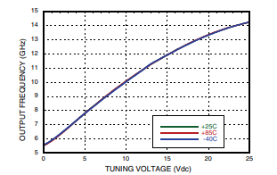
Frequency vs. Tuning Voltage, Vcc = +5V
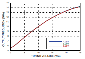
Frequency vs. Tuning Voltage, T = +25 °C
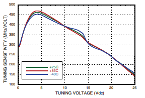
Sensitivity vs. Tuning Voltage, Vcc = +5V
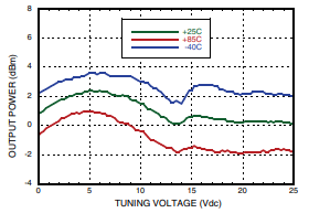
Output Power vs.
Tuning Voltage, Vcc = +5V
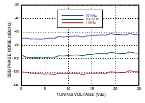
SSB Phase Noise vs. Tuning Voltage
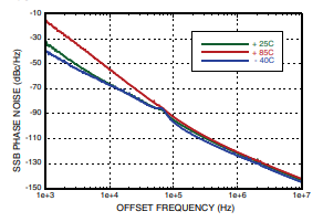
Typical SSB Phase Noise @ Vtune = +5V
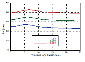
Supply Current vs. Vcc, T = 25 °C
Outline Drawing
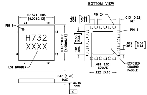
NOTES:
1. PACKAGE BODY MATERIAL: ALUMINA
2. LEAD AND GROUND PADDLE PLATING: GOLD FLASH OVER Ni.
3. DIMENSIONS ARE IN INCHES [MILLIMETERS].
4. LEAD SPACING TOLERANCE IS NON-CUMULATIVE.
5. PACKAGE WARP SHALL NOT EXCEED 0.05mm DATUM -C6. ALL GROUND LEADS AND GROUND PADDLE MUST BE SOLDERED
TO PCB RF GROUND.
Package Information
| Part Number | Package Body Material | Lead Finish | MSL Rating | Package Marking [2] |
|---|---|---|---|---|
| HMC732LC4B | Alumina, white | Gold over nickel | MSL3 [1] | H732 XXXX |
[1] Maximum peak reflow temperature: 260 °C
[2] XXXX = 4-digit lot number
Pin Descriptions
| Pin Number | Function | Description |
|---|---|---|
| 1–3, 5–11, 13, 16–24 | N/C | No connection. These pins may be tied to RF/DC ground without impacting performance. |
| 4 | Vtune | Control voltage and modulation input. Modulation bandwidth depends on the source impedance. (Refer to the application note “Determining the FM Bandwidth of a Wideband Varactor-Tuned VCO” for details.) |
| 12 | Vcc | Supply voltage: +5V |
| 14 | GND | Ground. The exposed metal paddle on the package bottom must also be connected to RF and DC ground. |
| 15 | RFOUT | RF output (AC-coupled). For proper operation, the load must maintain a VSWR ≤ 2.0:1 across the 0.01–14 GHz frequency range. |
Evaluation PCB
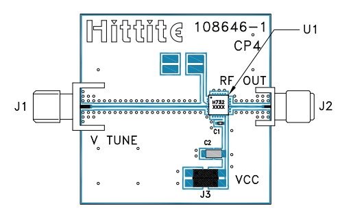
Bill of Materials – Evaluation PCB 108648 [1]
| Item | Description |
|---|---|
| J1 | RF Connector, SMA |
| J2 | RF Connector, SMA |
| J3 | DC Header |
| C1 | 1000 pF Capacitor, 0402 package |
| C2 | 4.7 µF Capacitor, Tantalum |
| U1 | HMC732LC4B VCO |
| PCB [2] | Evaluation Board 108646 |
[1] Reference this number when ordering the complete evaluation PCB.
[2] PCB substrate: Arlon 25FR or Rogers 4350.
PCB Design Guidelines
The application circuit board should follow standard RF design practices. Signal traces must maintain 50 Ω impedance, and both the package ground pins and the exposed paddle should be tied directly to the ground plane, as illustrated. Use a sufficient number of vias to connect the top and bottom ground planes for optimal performance.
An evaluation board, as shown, is available from Hittite upon request.
Conclusion
The HMC732LC4B is a compact, wideband MMIC VCO that combines low phase noise, wide tuning range, and low power consumption in a robust SMT package. With proper RF PCB design and grounding practices, it delivers reliable performance across industrial, medical, test, and military applications.

Christopher Anderson
Christopher Anderson has a Ph.D. in electrical engineering, focusing on power electronics. He’s been a Senior member of the IEEE Power Electronics Society since 2021. Right now, he works with the KPR Institute of Engineering and Technology in the U.S. He also writes detailed, top-notch articles about power electronics for business-to-business electronics platforms.
Subscribe to JMBom Electronics !


