


DS1267 Dual Digital Potentiometer Overview
Catalog
DESCRIPTIONFEATURESPIN DESCRIPTIONSOPERATIONDS1267 BLOCK DIAGRAMSTACKED CONFIGURATIONTIMING DIAGRAMSConclusionDESCRIPTION
The DS1267 Dual Digital Potentiometer integrates two solid-state potentiometers that are digitally controlled. Each potentiometer contains 256 resistive segments. The wiper can access tap points positioned between each segment and both ends of the resistor chain. The exact wiper location is determined by an 8-bit control value, which selects the tap point connected to the wiper output.
DS1267 Dual Digital Potentiometer
Control and communication with the chip are managed through a 3-wire serial interface, which allows both reading and adjusting the wiper position.
The two potentiometers can be linked in series (stacked) to achieve a higher overall resistance while maintaining the same resolution. For systems with multiple devices and a single processor, the DS1267 supports cascading or daisy-chaining, enabling control of multiple units through a single 3-wire bus.
The DS1267 is available in three resistance options: 10 kΩ, 50 kΩ, and 100 kΩ. Package choices include 14-pin DIP, 16-pin SOIC, and 20-pin TSSOP.
FEATURES
- Extremely low power usage with a quiet, pump-free design
- Dual digitally controlled potentiometers, each with 256 steps
- Serial interface allows both potentiometers to be set and read
- Potentiometers can be connected in series for higher overall resistance
- Available in 14-pin DIP, 16-pin SOIC, and 20-pin TSSOP packages
- Temperature-compensated resistive elements with ±0.3 LSB relative linearity
- Standard resistance options: DS1267-10: 10 kΩ DS1267-50: 50 kΩ DS1267-100: 100 kΩ
- Wide operating temperature range: –40°C to +85°C (industrial grade)
PIN DESCRIPTIONS
- L0, L1 – Low terminals of the resistors
- H0, H1 – High terminals of the resistors
- W0, W1 – Wiper terminals of the resistors
- VB – Substrate bias voltage
- SOUT – Output for stacked configuration
- RST – Reset input for the serial port
- DQ – Data input for the serial port
- CLK – Clock input for the serial port
- COUT – Cascade output port
- VCC – +5V power supply
- GND – Ground reference
- NC – No internal connection
PIN ASSIGNMENT
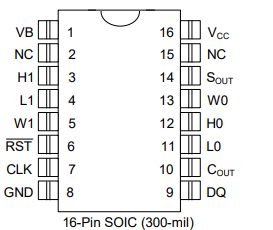
16-Pin SOIC (300-mil)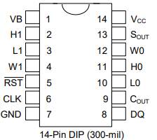
14-Pin DIP (300-mil)
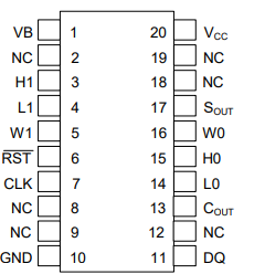
20-Pin TSSOP (173-mil)
OPERATION
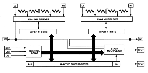
The DS1267 includes two 256-step potentiometers, with each wiper position defined by an 8-bit value. These two values, along with the stack select bit, are stored in a 17-bit I/O shift register when the device is powered on. A block diagram of the DS1267 is shown in Figure 1.
Communication and control are handled through a 3-wire serial interface, which connects to the device’s internal control logic. This interface uses three signals: RST, CLK, and DQ.
- RST: Enables the 3-wire serial interface. The DS1267 is active only when RST is high, and all communication must begin with RST set high.
- CLK: Provides the timing synchronization for data transfer.
- DQ: Transfers the potentiometer wiper settings and the stack select bit into the 17-bit I/O shift register.
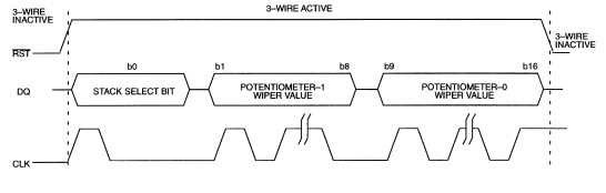
As shown in Figure 9(a), the 3-wire port is idle when RST is low. Communication starts when RST switches from low to high. Once active, data is shifted into the device on each low-to-high transition of the CLK signal. Serial timing requirements are shown in Figures 9(b)–9(c).
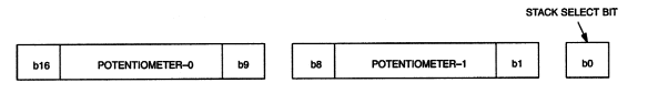
The 17-bit I/O shift register stores both 8-bit wiper positions and the stack select bit (see Figure 2):
- Bit 0: Stack select bit (details in “Stacked Configuration”).
- Bits 1–8: Wiper position for Potentiometer 1 (bit 1 = MSB, bit 8 = LSB).
- Bits 9–16: Wiper position for Potentiometer 0 (bit 9 = MSB, bit 16 = LSB).
DS1267 BLOCK DIAGRAM
DS1267 BLOCK DIAGRAM
I/O SHIFT REGISTER
I/O SHIFT REGISTER
Data transmission always starts with the stack select bit, followed by the wiper setting for potentiometer 1, and then the wiper setting for potentiometer 0.
When writing wiper position data to the DS1267, exactly 17 bits (or a whole-number multiple of 17 bits) must be transmitted. Sending fewer than 17 bits will leave the shift register incomplete and may cause incorrect wiper settings.
After completing a communication cycle, the RST signal should be driven low to prevent unintended changes in the shift register. Once RST goes low, the contents of the I/O shift register are transferred to the internal multiplexers, which update the wiper positions.
A new wiper setting only takes effect after the RST signal transitions to its inactive (low) state. At power-up, the DS1267 automatically initializes both wipers to the midpoint of the resistance range, corresponding to the binary value 1000 0000 (50%).
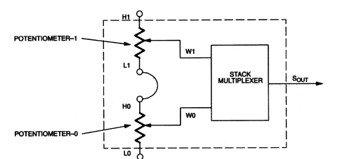
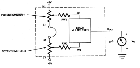
STACKED CONFIGURATION
The DS1267’s two potentiometers can be connected in series, as shown in Figure 3, in what’s called the stacked configuration. This setup effectively doubles the overall resistance and increases the resolution to 512 steps (9-bit resolution).
In this mode, the combined wiper output is available at the SOUT pin, which provides a multiplexed connection to either potentiometer-0’s wiper (W0) or potentiometer-1’s wiper (W1).
Which wiper is routed to SOUT is determined by the stack select bit (bit 0) in the 17-bit I/O shift register:
- If the stack select bit = 0, SOUT outputs the wiper of potentiometer-0.
- If the stack select bit = 1, SOUT outputs the wiper of potentiometer-1.
STACKED CONFIGURATION
CASCADE OPERATION
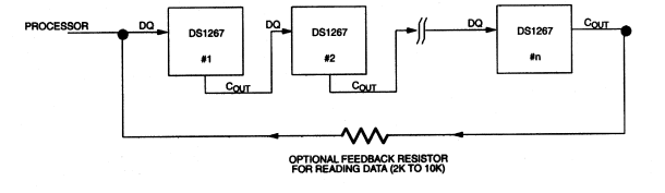
One of the DS1267’s key features is the ability to control multiple devices using a single processor. Several DS1267 chips can be connected in a daisy-chain configuration, as illustrated in Figure 4.
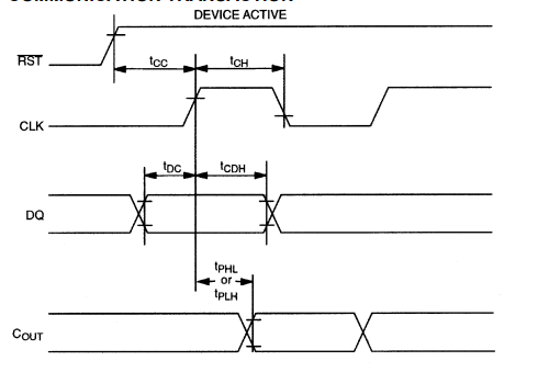
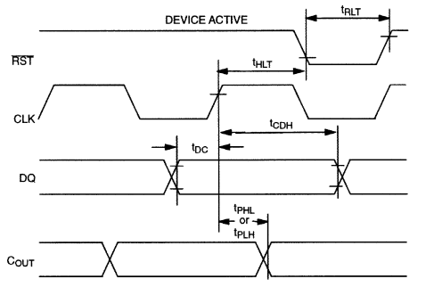
When a data bit is shifted into the I/O register of a DS1267, a corresponding bit appears at the COUT output, with a maximum propagation delay of 50 nanoseconds. During any transaction, the stack select bit is always the first bit shifted out.
The COUT pin remains active at all times, regardless of the RST signal state. This makes it possible to read the contents of the I/O shift register without altering its stored values.
CASCADING MULTIPLE DEVICES
CASCADE DATA FEEDBACK
The COUT output of one DS1267 can be connected to the DQ input of another, allowing multiple devices to be daisy-chained. In such a setup, the total number of bits transmitted equals 17 × the number of DS1267 devices in the chain.
An optional feedback resistor may be placed between the COUT pin of the last device and the DQ input of the first device. This allows the controlling processor to both write and read data, or to circulate data continuously through the chain. The feedback (or isolation) resistor should have a value between 1 kΩ and 10 kΩ.
When reading data through COUT and the isolation resistor, the DQ line is left floating by the processor. With RST driven high, bit 17 appears on the COUT pin and is looped back to DQ through the resistor. On each rising edge of CLK, this bit is shifted into the I/O register, while the next bit (bit 16, and so on) appears on COUT (and DQ of the next device). After 17 bits (or 17 × number of devices), the data has fully rotated back to its original position. When RST returns low, the I/O register values are reloaded into wiper-0, wiper-1, and the stack select bit, leaving them unchanged.
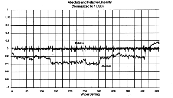
ABSOLUTE AND RELATIVE LINEARITY
- AL=VO(actual)−VO(expected)MIAL = \frac{V_O(\text{actual}) - V_O(\text{expected})}{MI}AL=MIVO(actual)−VO(expected)
- RL=VO(n+1)−VO(n)MIRL = \frac{V_O(n+1) - V_O(n)}{MI}RL=MIVO(n+1)−VO(n)
Figure 6 shows absolute and relative linearity versus wiper position at 25 °C. Typical specifications for the DS1267 are:
- Absolute linearity: ±0.75 MI
- Relative linearity: ±0.3 MI
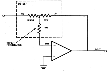
LINEARITY MEASUREMENT CONFIGURATION
LINEARITY MEASUREMENT CONFIGURATION
NOTE:
In this setup, a ±2% delta in total resistance R0 to R1 would cause a ±2.5 MI error.
DS1267 ABSOLUTE AND RELATIVE LINEARITY
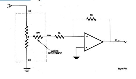
TYPICAL APPLICATION CONFIGURATIONS
Figures 7 and 8 illustrate two common ways to use the DS1267.
When the wiper terminal is connected to a high-impedance load, the effect of wiper resistance (which can range from 400 Ω to 1000 Ω, depending on voltage) is minimized.
- Av=−n255−n,n=0 to 255A_v = \frac{-n}{255-n}, \quad n = 0 \; \text{to} \; 255Av=255−n−n,n=0to255
- Figure 8 – Fixed Gain Attenuator The DS1267 is used to attenuate an input signal. In this setup, resistor R1 is selected to be much larger than the wiper resistance to minimize its influence on circuit performance.
INVERTING VARIABLE GAIN AMPLIFIER
FIX GAIN ATTENUATOR
ABSOLUTE MAXIMUM RATINGS*
- Voltage on any pin relative to ground (VB = GND): –0.1V to +7.0V
- Voltage on resistor pins when VB = –5.5V: –5.5V to +7.0V
- Voltage on VB: –5.5V to GND
- Operating temperature: –40°C to +85°C
- Storage temperature: –55°C to +125°C
- Soldering temperature: 260°C for 10 seconds
* These are stress ratings only. Operation at or beyond these limits is not guaranteed, and extended exposure may affect device reliability.
RECOMMENDED DC OPERATING CONDITIONS
(–40°C to +85°C; VCC = 5.0V ±10%)
| Parameter | Symbol | Min | Typ | Max | Units | Notes |
|---|---|---|---|---|---|---|
| Supply Voltage | VCC | 4.5 | — | 5.5 | V | 1 |
| Input Logic “1” | VIH | 2.0 | — | VCC+0.5 | V | 1 |
| Input Logic “0” | VIL | –0.5 | — | +0.8 | V | 1 |
| Substrate Bias | VB | –5.5 | — | GND | V | 1 |
| Resistor Inputs (L,H,W) | — | VB–0.5 | — | VCC+0.5 | V | 2 |
DC ELECTRICAL CHARACTERISTICS
(–40°C to +85°C; VCC = 5.0V ±10%)
| Parameter | Symbol | Min | Typ | Max | Units | Notes |
|---|---|---|---|---|---|---|
| Supply Current | ICC | 22 | — | 650 | µA | 9 |
| Input Leakage Current | ILI | –1 | — | +1 | µA | — |
| Wiper Resistance | RW | 400 | — | 1000 | Ω | 5 |
| Wiper Current | IW | — | — | 1 | mA | — |
| Output Leakage Current | ILO | –1 | — | +1 | µA | — |
| Logic “1” Output @ 2.4V | IOH | — | — | –1 | mA | 7 |
| Logic “0” Output @ 0.4V | IOL | — | — | 4 | mA | 7 |
| Standby Current | ISTBY | — | 22 | — | µA | 5 |
ANALOG RESISTOR CHARACTERISTICS
(–40°C to +85°C; VCC = 5.0V ±10%)
| Parameter | Symbol | Min | Typ | Max | Units | Notes |
|---|---|---|---|---|---|---|
| End-to-End Resistor Tolerance | — | –20 | — | +20 | % | 10 |
| Absolute Linearity | — | — | — | ±0.75 | LDB | 3 |
| Relative Linearity | — | — | — | ±0.3 | LDB | 4 |
| –3 dB Cutoff Frequency | FCUTOFF | — | — | — | Hz | 6 |
| Temperature Coefficient | — | — | 750 | — | ppm/°C | — |
CAPACITANCE
(TA = 25°C)
| Parameter | Symbol | Typ | Units | Notes |
|---|---|---|---|---|
| Input Capacitance | CIN | 5 | pF | — |
| Output Capacitance | COUT | 7 | pF | — |
AC ELECTRICAL CHARACTERISTICS
(–40°C to +85°C; VCC = 5.0V ±10%)
| Parameter | Symbol | Min | Typ | Max | Units | Notes |
|---|---|---|---|---|---|---|
| CLK Frequency | fCLK | DC | — | 10 | MHz | 8 |
| CLK Pulse Width | tCH | 50 | — | — | ns | 8 |
| Data Setup Time | tDC | 30 | — | — | ns | 8 |
| Data Hold Time | tCDH | 10 | — | — | ns | 8 |
| Propagation Delay Low → High | tPLH | — | — | 50 | ns | 8 |
| Propagation Delay High → Low | tPHL | — | — | 50 | ns | 8 |
| RST High → CLK High | tCC | — | — | 50 | ns | 8 |
| RST Low → CLK High | tHLT | — | — | 50 | ns | 8 |
| RST Inactive | tRLT | — | — | 125 | ns | 8 |
| CLK Rise/Fall Time | tCR | — | — | 50 | ns | 8 |
NOTES:
- All voltages are referenced to ground.
- Resistor inputs cannot exceed the substrate bias voltage (VB) in the negative direction.
- Absolute linearity defines the deviation of the actual wiper voltage from the expected voltage based on wiper position. Device test limits: ±1.6 LSB.
4. Relative linearity measures the voltage difference between consecutive tap positions. Device test limits: ±0.5 LSB.
5. Typical values are specified for TA = 25°C with nominal supply voltage.
6. The –3 dB cutoff frequency depends on total potentiometer resistance:
- DS1267-010: 1 MHz
- DS1267-050: 200 kHz
- DS1267-100: 100 kHz
7.COUT remains active regardless of the RST signal state.
8.Timing diagrams and serial interface details are shown in Figures 9(a), 9(b), and 9(c).
9.Additional reference data is provided in Figure 11.
10.Some specifications are valid only at 25°C.
TIMING DIAGRAMS
3-WIRE SERIAL INTERFACE GENERAL OVERVIEW
START OF COMMUNICATION TRANSACTION
END OF COMMUNICATION TRANSACTION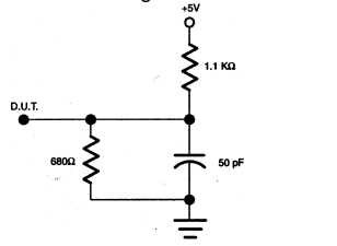
DIGITAL OUTPUT LOAD SCHEMATIC
TYPICAL SUPPLY CURENT VS. SERIAL CLOCK RATE
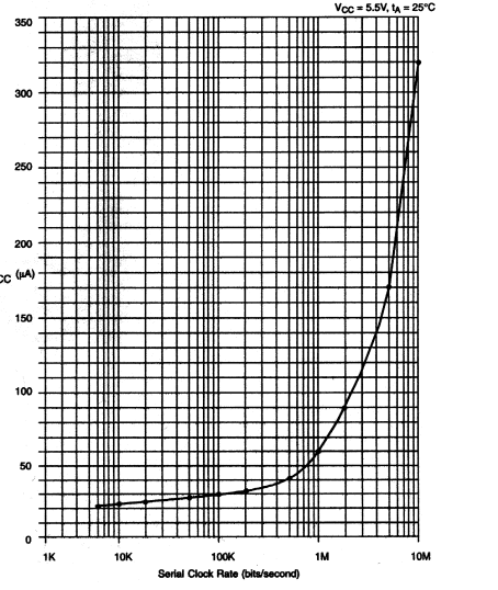
TYPICAL SUPPLY CURENT VS. SERIAL CLOCK RATE
Conclusion
The DS1267 is a versatile dual digital potentiometer offering precise, digitally controlled resistance with 256 positions per potentiometer. Its features—such as stacking, cascading, low power consumption, and serial interface control—enable flexible configuration in both single- and multi-device systems. The device provides high linearity, reliable performance across a wide temperature range, and compatibility with standard IC packages, making it suitable for applications like variable gain amplifiers and signal attenuation.

Christopher Anderson
Christopher Anderson has a Ph.D. in electrical engineering, focusing on power electronics. He’s been a Senior member of the IEEE Power Electronics Society since 2021. Right now, he works with the KPR Institute of Engineering and Technology in the U.S. He also writes detailed, top-notch articles about power electronics for business-to-business electronics platforms.
Subscribe to JMBom Electronics !


