


LT3042: High-Performance Low-Noise Linear Regulator
Catalog
DESCRIPTIONFEATURESAPPLICATIONSLT3042 PIN CONFIGURATIONAPPLICATIONS INFORMATIONTypical Output Voltages and Corresponding RSET ValuesAPPLICATIONS INFORMATIONConclusionDESCRIPTION
The LT®3042 is a high-performance, low dropout linear regulator that uses LTC’s ultra-low noise and ultra-high PSRR design, making it ideal for sensitive RF applications.
Built with a precision current reference followed by a high-performance voltage buffer, the LT3042 can be easily connected in parallel to further lower noise, increase output current, and improve heat dissipation across the PCB.
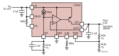
TYPICAL APPLICATION
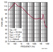
Power Supply Ripple Rejection
It delivers up to 200mA with a typical dropout voltage of just 350mV. The regulator operates with a low quiescent current of about 2mA, which falls to under 1µA in shutdown mode. Its wide output voltage range (0V to 15V) with unity-gain operation ensures nearly constant output noise, PSRR, bandwidth, and load regulation, regardless of the set output voltage.
Additional features include programmable current limit, fast startup, and a programmable “power good” signal to indicate stable output regulation.
The LT3042 remains stable with as little as a 4.7µF ceramic output capacitor. Built-in protections include reverse battery protection, reverse current blocking, internal current limiting with foldback, and thermal shutdown with hysteresis. The LT3042 is offered in thermally enhanced 10-Lead MSOP and compact 3mm × 3mm DFN packages.
FEATURES
- Extremely low RMS noise: 0.8µVRMS (10Hz to 100kHz)
- Very low spot noise: 2nV/√Hz at 10kHz
- Exceptional PSRR: 79dB at 1MHz
- Output current up to 200mA
- Wide input voltage range: 1.8V to 20V
- Single capacitor enhances both noise and PSRR
- SET pin current of 100µA with ±1% initial accuracy
- Output voltage set with a single resistor
- High bandwidth: 1MHz
- Adjustable current limit
- Low dropout: 350mV
- Output voltage range: 0V to 15V
- Programmable “power good” indication
- Fast start-up response
- Precision enable/UVLO control
- Can be paralleled for lower noise and higher current output
- Built-in current limit with foldback
- Stable with as little as 4.7µF ceramic output capacitor
- Protection against reverse battery and reverse current
- Available in 10-Lead MSOP and compact 3mm × 3mm DFN packages
APPLICATIONS
- RF power supplies: PLLs, VCOs, mixers, LNAs
- Ultra-low noise instrumentation
- High-speed, high-precision data converters
- Medical equipment: imaging, diagnostics
- Precision power supplies
- Post-regulation for switching power supplies
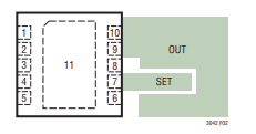
LT3042 PIN CONFIGURATION
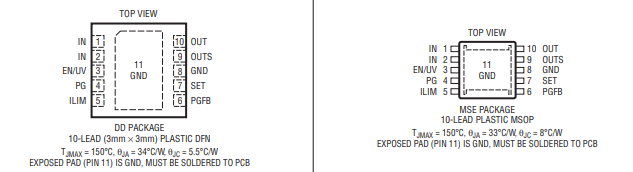
LT3042 PIN CONFIGURATION
APPLICATIONS INFORMATION
The LT3042 is a high-performance, low dropout linear regulator that uses LTC’s ultra-low noise design (2nV/√Hz at 10kHz) and ultra-high PSRR (79dB at 1MHz), making it well-suited for powering noise-sensitive circuits. Built as a precision current source paired with a rail-to-rail voltage buffer, the LT3042 can be paralleled to further lower noise, boost output current, and improve heat distribution on the PCB. It also includes programmable current limit, fast start-up, and a programmable power-good signal.
The LT3042 is user-friendly and comes with all the essential protection features expected in high-performance regulators. These include short-circuit protection, safe operating area protection, reverse battery protection, reverse current protection, and thermal shutdown with hysteresis.
Output Voltage
The LT3042 uses a precision 100µA current source that flows out of the SET pin, which also connects to the inverting input of the error amplifier. As shown in Figure 1, placing a resistor between SET and ground generates a reference voltage for the error amplifier. This voltage is simply the product of the SET pin current and the resistor value. The error amplifier, configured for unity gain, provides a low-impedance version of this voltage at its non-inverting input (the OUTS pin), which is externally connected to the OUT pin.
Thanks to its rail-to-rail error amplifier and current reference, the LT3042 supports a wide output voltage range from 0V (using a 0Ω resistor) up to VIN minus dropout — with a maximum of 15V. For outputs between 0V and 0.6V, a PNP-based input pair is active; for outputs above 1.3V, an NPN-based input pair takes over. Between 0.6V and 1.3V, the transition between the two input stages is smooth. The NPN-based input pair provides the best overall performance, but for detailed specifications such as offset voltage, SET pin current, output noise, and PSRR behavior, refer to the Electrical Characteristics Table. Common output voltages and their corresponding 1% RSET resistor values are summarized in Table 1.
Typical Output Voltages and Corresponding RSET Values
| VOUT (V) | RSET (kΩ) |
|---|---|
| 2.5 | 24.9 |
| 3.3 | 33.2 |
| 5.0 | 49.9 |
| 12.0 | 121 |
| 15.0 | 150 |
The key advantage of using a current reference instead of the conventional voltage reference is that the regulator always operates in a unity-gain configuration, regardless of the programmed output voltage. This design ensures that loop gain, frequency response, and bandwidth remain constant across the entire output voltage range. As a result, parameters such as noise, PSRR, and transient response do not vary with output voltage. Furthermore, since the error amplifier’s gain is not used to scale the SET pin voltage to higher outputs, load regulation can be specified much more tightly—within hundreds of microvolts rather than as a percentage of the output voltage.
Because the zero-TC current source is extremely accurate, the precision of the SET pin resistor becomes the main factor in achieving high accuracy. Therefore, a precision resistor must be used. Any leakage paths to or from the SET pin can introduce errors in the output voltage. To minimize this, high-quality insulation materials (such as Teflon or Kel-F) are recommended, and insulating surfaces should be thoroughly cleaned to remove flux and other residues. In high-humidity environments, applying a surface coating around the SET pin may be necessary to provide a moisture barrier.
To further reduce leakage, it is best to surround the SET pin with a guard ring held at a potential close to the SET pin—ideally tied to the OUT pin. Guarding on both sides of the PCB is recommended. The effectiveness of bulk leakage reduction depends on the width of the guard ring. For example, leakage currents of just 100nA into or out of the SET pin can cause a 0.1% error in the reference voltage. When combined with other leakage sources, such errors can significantly affect output voltage accuracy, especially across wide temperature ranges. Figure 2 shows a typical guard ring layout.
Guard Ring Layout
Connections for Stability
Because the SET pin is a high-impedance node, it can pick up unwanted signals that may cause instability. This issue is most noticeable when operating with the minimum output capacitor under heavy load conditions. Adding a small bypass capacitor from the SET pin to ground resolves this — typically 10nF is sufficient.
For applications that demand higher accuracy or adjustable output voltages, the SET pin can also be driven by an external precision voltage source capable of sinking 100µA. In this setup, connecting a voltage reference directly to the SET pin eliminates output errors caused by the reference current and resistor tolerances.
Output Sensing and Stability
The LT3042 provides Kelvin sense connections for optimal performance: the OUTS pin senses the output voltage directly, while the ground side of the SET resistor connects to the load’s ground.
Because the LT3042 is designed for very high PSRR, its bandwidth is relatively high (~1MHz). This is close to the self-resonant frequency of a typical 4.7µF ceramic output capacitor (~2.3MHz for 1206 case size). To prevent additional impedance (ESR/ESL) from degrading stability, PCB parasitics must be minimized. As shown in Figure 3, connect the OUTS pin directly to COUT, tie the GND side of CSET directly to the GND side of COUT, and place the GND connections of CIN and COUT close together. While the LT3042 will not oscillate if the layout is suboptimal, poor layout may reduce phase/gain margin, noise performance, and PSRR.
Stability and Output Capacitance
The LT3042 requires an output capacitor for stable operation. Because of its high bandwidth, low-ESR and low-ESL ceramic capacitors are recommended. Stability requires a minimum 4.7µF capacitor with ESR <50mΩ and ESL <2nH.
Although using larger capacitors provides little improvement in noise or PSRR (since bandwidth decreases with increasing capacitance), they can reduce peak output deviations during load transients. Also note that any bypass capacitors used to decouple powered components contribute to the effective output capacitance.
Care must be taken when selecting ceramic capacitor dielectrics. Common types include Z5U, Y5V, X5R, and X7R. While Z5U and Y5V provide high capacitance in small sizes, their capacitance varies greatly with voltage and temperature — for instance, a 16V 10µF Y5V capacitor may deliver only 1µF–2µF under bias. X5R and X7R capacitors are more stable and therefore recommended for LT3042 applications. X7R offers better temperature stability, while X5R is lower cost and available in higher values. Even so, capacitance reduction under DC bias can still be significant, so verifying actual capacitance at operating voltage is strongly advised. Larger case sizes typically show better bias characteristics, as illustrated in Figure 6.
High Vibration Environments
Capacitor behavior is also affected by mechanical stress. Certain ceramic capacitors exhibit piezoelectric effects, generating voltage when exposed to vibration or thermal transients, much like a piezoelectric microphone.
In LT3042 applications, three capacitors may contribute to piezoelectric noise: the output capacitor, the input capacitor, and the SET pin capacitor. Thanks to the LT3042’s low output impedance and high PSRR, noise from the output and input capacitors is negligible. However, the high impedance of the SET pin makes it very sensitive to piezoelectric effects, which can introduce output noise in the hundreds of microvolts range.
To avoid this, use a capacitor type without piezoelectric response at the SET pin, such as tantalum, film, or electrolytic (though electrolytics may have higher 1/f noise). Surface-mount capacitors are strongly recommended.
Stability and Input Capacitance
The LT3042 remains stable with a minimum of 4.7µF input capacitance, preferably a low-ESR ceramic capacitor.
When long wires connect the supply to the LT3042 input and ground, a small input capacitor together with large load currents can form a resonant LC tank circuit with the wire inductance, leading to instability. Importantly, this effect comes from the wiring—not from instability of the LT3042 itself.
Wire self-inductance is mainly a function of length; diameter has less effect. For example, one foot of 30-AWG wire has about 465nH of inductance.
To reduce wire inductance:
- Split current into parallel conductors placed apart (up to 50% reduction).
- Place forward and return conductors (input and ground) very close together. Two 30-AWG wires spaced 0.02" apart reduce inductance to ~1/5 of a single wire.
If a nearby battery powers the LT3042, the 4.7µF capacitor is sufficient. For remote supplies, increase input capacitance using the rule of thumb: +1µF per 8 inches of wire, in addition to the 4.7µF minimum.
Adding output capacitance also improves stability, but far less effectively than input capacitance. Series resistance between the source and LT3042 input (0.1Ω–0.5Ω) can also damp the LC resonance, though it increases dropout voltage. A better approach is to use a tantalum or electrolytic capacitor (with higher ESR) in parallel with the ceramic input capacitor.
PSRR and Input Capacitance
When post-regulating a switching converter, the input capacitor at the LT3042 allows switching ripple currents to flow near the regulator. These high-frequency AC currents (at the switcher frequency, e.g. ~1MHz) generate magnetic fields that couple into the LT3042 and reduce its effective PSRR by more than 30dB at 1MHz.
This effect comes from the PCB parasitics and switching current loops, and persists even if the LT3042 is removed from the board. Conventional LDOs (with lower PSRR) are less sensitive, but the LT3042’s ultrahigh PSRR demands careful PCB layout.
One option is to omit the input capacitor, provided the switching regulator output capacitor is >1" away from the LT3042. However, if the pre-regulator is more than a few inches away, the LT3042 input may oscillate. Since input bypassing is standard practice, this is a limited solution.
A better approach is to follow the DC2246B demo board layout, which uses magnetic field cancellation to preserve PSRR performance even with an input capacitor present.
Filtering High-Frequency Spikes
The LT3042 suppresses switching noise in the 100kHz–4MHz range very effectively. However, very high frequency spikes (hundreds of MHz) from the switcher’s fast transitions can pass through, since they lie beyond the regulator’s bandwidth.
The output capacitor helps absorb these spikes, but its ESL limits performance. A ferrite bead or even a short PCB trace inductance (~0.5”) between the switcher output and LT3042 input can serve as an LC filter to attenuate these spikes.
Output Noise
Unlike conventional regulators, the LT3042 uses a 100µA current reference (not a voltage reference) with noise of ~20pA/√Hz (≈6nARMS, 10Hz–100kHz). The resulting voltage noise is set by:
- Current noise × RSET
- Summed with the error amplifier noise
- Plus thermal noise of RSET (√4kTR).
Because the LT3042 operates as a unity-gain buffer, there is no noise gain from a divider network. Bypassing the SET pin resistor with a capacitor makes output noise independent of VOUT, leaving only the error amplifier contribution (~2nV/√Hz, 10kHz–1MHz; ~0.8µVRMS over 10Hz–100kHz with 4.7µF CSET).
Noise can be reduced further by paralleling regulators: N devices reduce noise by √N.
SET Pin Bypass Capacitor: Noise, PSRR, Transient, and Soft-Start
Adding a capacitor from SET to ground improves:
- Noise (lower RMS levels)
- PSRR (especially at high frequency)
- Transient performance
- Soft-start behavior
The soft-start time is given by:tSS≈2.3⋅RSET⋅CSETt_{SS} \approx 2.3 \cdot R_{SET} \cdot C_{SET}tSS≈2.3⋅RSET⋅CSET
(with fast-start disabled).
Caution: leakage current through CSET directly degrades DC regulation (100nA leakage = 0.1% error). Use low-leakage ceramic capacitors.
Fast Start-Up
For ultra-low noise (low 1/f, <100Hz), CSET values up to 22µF may be used. Normally this would slow start-up significantly, but the LT3042 includes fast-start circuitry: the SET pin current temporarily increases to ~2mA until PGFB exceeds 300mV (unless in current limit, dropout, thermal shutdown, or low VIN).
To disable fast start-up, tie PGFB to IN (or OUT if VOUT > 300mV). Note: this also disables the power-good function.
APPLICATIONS INFORMATION
ENABLE/UVLO
The EN/UV pin controls whether the regulator is active or in micropower shutdown. The LT3042 features a precise 1.24V turn-on threshold with 170mV hysteresis. By combining this pin with a resistor divider from the input supply, you can set an accurate undervoltage lockout (UVLO) level.
When calculating the divider, account for the EN/UV pin current (IEN) listed in the Electrical Characteristics table:VIN(UVLO)=1.24V⋅(1+REN2REN1)+IEN⋅REN2V_{IN(UVLO)} = 1.24V \cdot \left(1 + \frac{R_{EN2}}{R_{EN1}}\right) + I_{EN} \cdot R_{EN2}VIN(UVLO)=1.24V⋅(1+REN1REN2)+IEN⋅REN2
If REN1 is less than 100kΩ, IEN can be ignored. If the feature is unused, tie EN/UV directly to IN.
Programmable Power Good
As shown in the Block Diagram, the power good threshold can be set by two external resistors, RPG2 and RPG1:VOUT(PG_THRESHOLD)=0.3V⋅(1+RPG2RPG1)+IPGFB⋅RPG2V_{OUT(PG\_THRESHOLD)} = 0.3V \cdot \left(1 + \frac{R_{PG2}}{R_{PG1}}\right) + I_{PGFB} \cdot R_{PG2}VOUT(PG_THRESHOLD)=0.3V⋅(1+RPG1RPG2)+IPGFB⋅RPG2
When the PGFB pin rises above 300mV, the open-collector PG pin de-asserts (goes high impedance). The comparator includes 7mV hysteresis and 5µs deglitching.
The PGFB pin current (IPGFB) must be considered when sizing the divider, though it can be ignored if RPG1 is less than 30kΩ. If power good is unused, simply leave PG floating. Note that this function, along with fast start-up, is unavailable for output voltages below 300mV or when the device is in shutdown.
Externally Programmable Current Limit
The ILIM pin sets the current limit. Its threshold is 300mV, and a resistor from ILIM to GND defines the maximum current:Current Limit=125mA⋅kΩRILIM\text{Current Limit} = \frac{125mA \cdot k\Omega}{R_{ILIM}}Current Limit=RILIM125mA⋅kΩ
- 1kΩ → 125mA limit
- 2kΩ → 62.5mA limit
For best accuracy, Kelvin-connect this resistor directly to the GND pin.
If the IN-to-OUT differential exceeds 12V, internal foldback reduces the current limit to keep the LT3042 safe, overriding the external setting.
The ILIM pin also sources a current proportional to the output (1:400), so it can act as a current monitor with a 0–300mV range. If neither feature is needed, tie ILIM to GND.
Output Overshoot Recovery
During a load step from full load to no load, the output can overshoot before the regulator adjusts. Since the output capacitor has little load to discharge into, recovery can take time.
To address this, the LT3042 includes overshoot recovery circuitry. When OUTS exceeds SET, a ~4mA current sink activates to discharge the output capacitor. This function is disabled if VIN < 2.5V or VOUT < 1.5V.
If an external circuit forces OUTS above SET, the sink will remain on until OUTS is released back to normal.
Direct Paralleling for Higher Current
To increase output current, multiple LT3042s can be paralleled:
- Tie all SET pins together.
- Tie all IN pins together.
- Connect OUT pins together using short PCB traces as ballast resistors to balance currents.
Conclusion
The LT3042 is a high-performance, ultralow-noise, and ultrahigh-PSRR linear regulator designed for precision, noise-sensitive applications. Its architecture—including a 100µA current reference, rail-to-rail error amplifier, and unity-gain follower design—ensures consistent noise, PSRR, and transient performance independent of output voltage. Features such as programmable current limit, fast start-up, EN/UV control, and programmable power-good enhance flexibility and protection. Careful attention to input/output capacitors, SET pin bypassing, PCB layout, and wiring minimizes noise, maintains stability, and maximizes performance. Multiple LT3042s can be paralleled for higher current with balanced load sharing. Overall, the LT3042 combines precision, stability, and versatility, making it ideal for low-noise RF, instrumentation, medical, and high-accuracy power supply applications.

Amanda Miller
Amanda Miller is a senior electronics engineer with 6 years of experience. She focuses on studying resistors, transistors, and package design in detail. Her deep knowledge helps her bring innovation and high standards to the electronics industry.
Subscribe to JMBom Electronics !


