


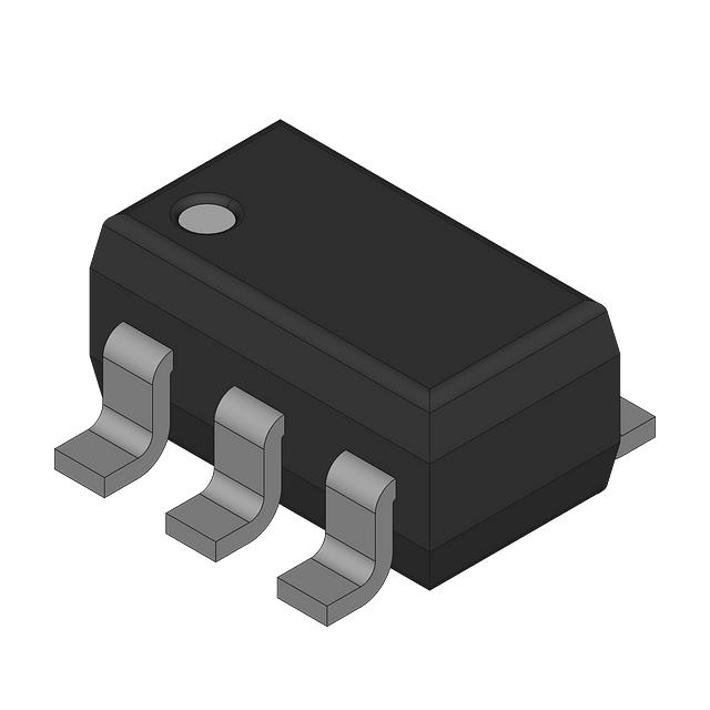
MIC5207 180mA Ultra-Low Noise LDO Regulator
Catalog
FeaturesApplicationsTypical ApplicationOrdering InformationPin ConfigurationPin DescriptionBlock DiagramsApplication InformationAdjustable Regulator ApplicationsPackage InformationConclusionOverview
The MIC5207 is a high-efficiency linear voltage regulator that delivers an ultra-low-noise output, exceptionally low dropout voltage (typically 17mV at light loads and 165mV at 150mA), and minimal ground current (720μA at 100mA output). It ensures better than 3% initial accuracy.
MIC5207 180mA Ultra-Low Noise LDO Regulator
Specially designed for portable, battery-powered devices, the MIC5207 features a CMOS- and TTL-compatible enable/shutdown control pin. In shutdown mode, its power consumption nearly drops to zero.
Notable features of the MIC5207 include a reference bypass pin for enhanced noise reduction, reverse-battery protection, current limiting, and thermal shutdown.
The MIC5207 is offered in both fixed and adjustable output voltage options, housed in a compact SOT-23-5 package. For details, please contact Micrel.
For other low-dropout regulators compatible with ceramic output capacitors, see the μCap MIC5245/6/7 series.
Features
- Ultra-low noise output
- High accuracy for output voltage
- Guaranteed 180mA output current
- Low quiescent current consumption
- Very low dropout voltage
- Excellent load and line regulation
- Minimal temperature coefficient
- Built-in current and thermal protection
- Reverse-battery safeguard
- Near-zero current in shutdown mode
- Logic-level controlled enable function
Applications
- Mobile and cellular phones
- Laptops, notebooks, and handheld PCs
- Battery-operated devices
- PCMCIA VCC and VPP regulation/switching
- Consumer and personal electronics
- Post-regulation for SMPS and DC-DC modules
- High-efficiency linear power supplies
Typical Application
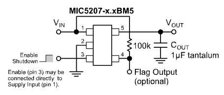
Battery-Powered Regulator Application
Ordering Information
| Part Number | Marking | Output Voltage* | Junction Temp. Range | Package | Lead Finish |
|---|---|---|---|---|---|
| MIC5207-1.8BD5 | NE18 | 1.8V | –40°C to +125°C | 5-Pin Thin SOT-23 | Standard |
| MIC5207BM5 | LEAA | Adjustable | –40°C to +125°C | 5-Pin SOT-23 | Standard |
| MIC5207-1.8BM5 | LE18 | 1.8V | –40°C to +125°C | 5-Pin SOT-23 | Standard |
| MIC5207-2.5BM5 | LE25 | 2.5V | –40°C to +125°C | 5-Pin SOT-23 | Standard |
| MIC5207-2.8BM5 | LE28 | 2.8V | –40°C to +125°C | 5-Pin SOT-23 | Standard |
| MIC5207-3.0BM5 | LE30 | 3.0V | –40°C to +125°C | 5-Pin SOT-23 | Standard |
| MIC5207-3.2BM5 | LE32 | 3.2V | –40°C to +125°C | 5-Pin SOT-23 | Standard |
| MIC5207-3.3BM5 | LE33 | 3.3V | –40°C to +125°C | 5-Pin SOT-23 | Standard |
| MIC5207-3.6BM5 | LE36 | 3.6V | –40°C to +125°C | 5-Pin SOT-23 | Standard |
| MIC5207-3.8BM5 | LE38 | 3.8V | –40°C to +125°C | 5-Pin SOT-23 | Standard |
| MIC5207-4.0BM5 | LE40 | 4.0V | –40°C to +125°C | 5-Pin SOT-23 | Standard |
| MIC5207-5.0BM5 | LE50 | 5.0V | –40°C to +125°C | 5-Pin SOT-23 | Standard |
| MIC5207-3.3BZ*** | -- | 3.3V | –40°C to +125°C | 3-Pin TO-92 | Standard |
| MIC5207-1.8YD5 | NE18** | 1.8V | –40°C to +125°C | 5-Pin Thin SOT-23 | Pb-Free |
| MIC5207YM5 | LEAA** | Adjustable | –40°C to +125°C | 5-Pin SOT-23 | Pb-Free |
| MIC5207-1.8YM5 | LE18** | 1.8V | –40°C to +125°C | 5-Pin SOT-23 | Pb-Free |
| MIC5207-2.5YM5 | LE25** | 2.5V | –40°C to +125°C | 5-Pin SOT-23 | Pb-Free |
| MIC5207-2.8YM5 | LE28** | 2.8V | –40°C to +125°C | 5-Pin SOT-23 | Pb-Free |
| MIC5207-2.9YM5 | LE29** | 2.9V | –40°C to +125°C | 5-Pin SOT-23 | Pb-Free |
| MIC5207-3.0YM5 | LE30** | 3.0V | –40°C to +125°C | 5-Pin SOT-23 | Pb-Free |
| MIC5207-3.1YM5 | LE31** | 3.1V | –40°C to +125°C | 5-Pin SOT-23 | Pb-Free |
| MIC5207-3.2YM5 | LE32** | 3.2V | –40°C to +125°C | 5-Pin SOT-23 | Pb-Free |
| MIC5207-3.3YM5 | LE33** | 3.3V | –40°C to +125°C | 5-Pin SOT-23 | Pb-Free |
| MIC5207-3.6YM5 | LE36** | 3.6V | –40°C to +125°C | 5-Pin SOT-23 | Pb-Free |
| MIC5207-3.8YM5 | LE38** | 3.8V | –40°C to +125°C | 5-Pin SOT-23 | Pb-Free |
| MIC5207-4.0YM5 | LE40** | 4.0V | –40°C to +125°C | 5-Pin SOT-23 | Pb-Free |
| MIC5207-5.0YM5 | LE50** | 5.0V | –40°C to +125°C | 5-Pin SOT-23 | Pb-Free |
| MIC5207-3.3YZ*** | -- | 3.3V | –40°C to +125°C | 3-Pin TO-92 | Pb-Free |
Other output voltages available. Contact Micrel for more information.
The underscore symbol ( __ ) may not be shown to scale.
TO-92 package discontinuance notice issued September 2007. End-of-life buy available until December 31, 2007. Please contact the factory for additional details.
Pin Configuration
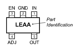
MIC5207BM5/YM5 (M5)(Adjustable Voltage)
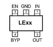
MIC5207-x.xBM5/YM5 (M5)
MIC5207-x.xBD5/YD5 (D5)
(Fixed Voltage)
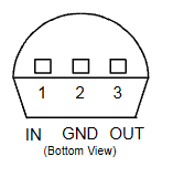
MIC5207-x.xBZ/YZ (Z)(Fixed Voltage)
Pin Description
| Pin Number (SOT-23-5) | Pin Number (TO-92) | Pin Name | Function |
|---|---|---|---|
| 1 | 1 | IN | Supply input |
| 2 | 2 | GND | Ground connection |
| 3 | — | EN | Enable/Shutdown control (Input). CMOS-compatible. Logic high = enable, logic low or open = shutdown. Do not leave floating. |
| 4 (fixed version) | — | BYP | Reference bypass. Connect a 470pF capacitor to GND to minimize output noise. Can be left unconnected. For 1.8V or 2.5V operation, refer to “Applications Information.” |
| 4 (adjustable version) | — | ADJ | Adjust input. Feedback input for adjustable regulator. Connect to an external resistor divider. |
| 5 | 3 | OUT | Regulator output |
Absolute Maximum Ratings (1)
- Supply Input Voltage (VIN): –20V to +20V
- Enable Input Voltage (VEN): –20V to +20V
- Power Dissipation (PD): Internally limited (3)
- Lead Temperature (soldering, 5 sec): 260°C
- Junction Temperature (TJ): All versions except 1.8V: –40°C to +125°C 1.8V version only: 0°C to +125°C
- Storage Temperature (TS): –65°C to +150°C
Operating Ratings (2)
- Supply Input Voltage (VIN): +2.5V to +16V
- Enable Input Voltage (VEN): 0V to VIN
- Junction Temperature (TJ): All versions except 1.8V: –40°C to +125°C 1.8V version only: 0°C to +125°C
- Thermal Resistance (θJA): See Note 3 MSOP-8 (θJA): (3
Electrical Characteristics
Conditions: VIN = VOUT + 1V; IL = 100μA; CL = 1.0μF; VEN ≥ 2.0V; TJ = 25°C. Bold values apply over –40°C < TJ < +125°C (0°C < TJ < +125°C for 1.8V version), unless otherwise specified.
| Symbol | Parameter | Test Conditions | Min | Typ | Max | Units |
|---|---|---|---|---|---|---|
| VO | Output Voltage Accuracy | Variation from nominal VOUT | –3 –4 | — | 3 4 | % |
| ΔVO/ΔT | Output Voltage Temperature Coefficient | Note 4 | — | 40 | — | ppm/°C |
| ΔVO/VO | Line Regulation | VIN = VOUT + 1V → 16V | 0.005 | 0.05 | 0.10 | %/V |
| ΔVO/VO | Load Regulation | IL = 0.1mA → 150mA, Note 5 | 0.05 | 0.5 | 0.7 | % |
| VIN – VO | Dropout Voltage, Note 6 | IL = 100μA | 17 | 60 | 300 | mV |
| IL = 50mA | 115 | 140 | 175 | mV | ||
| IL = 100mA | 165 | 250 | 280 | mV | ||
| IL = 150mA | — | 325 | 400 | mV | ||
| IGND | Quiescent Current | VEN ≤ 0.4V (shutdown) | 0.01 | 1 | 5 | μA |
| VEN ≤ 0.18V (shutdown) | — | — | — | μA | ||
| IGND | Ground Pin Current, Note 7 | VEN ≥ 2.0V, IL = 100μA | 80 | 130 | 200 | μA |
| IL = 50mA | 350 | 650 | 1100 | μA | ||
| IL = 100mA | 720 | 900 | 2000 | μA | ||
| IL = 150mA | 1800 | 2500 | 3000 | μA | ||
| PSRR | Ripple Rejection | — | — | 75 | — | dB |
| ILIMIT | Current Limit | VOUT = 0V | 320 | 500 | — | mA |
| ΔVO/ΔPD | Thermal Regulation | Note 8 | — | 0.05 | — | %/W |
| eNO | Output Noise | IL = 50mA; CL = 2.2μF; 470pF bypass capacitor (BYP → GND) | — | 260 | — | nV/√Hz |
Enable Input Characteristics
Conditions: Unless otherwise specified.
| Symbol | Parameter | Condition | Min | Typ | Max | Units |
|---|---|---|---|---|---|---|
| VIL | Enable Input Logic-Low Voltage | Regulator shutdown | — | — | 0.4 0.18 | V |
| VIH | Enable Input Logic-High Voltage | Regulator enable | 2.0 | — | — | V |
| IIL | Enable Input Current | VIL ≤ 0.4V | 0.01 | — | 20 | μA |
| VIL ≤ 0.18V | — | — | 25 | μA | ||
| IIH | Enable Input Current | VIH ≥ 2.0V | –1 | — | — | μA |
| VIH ≥ 2.0V | –2 | — | — | μA |
Notes:
- Exceeding the absolute maximum ratings may permanently damage the device.
- The regulator is not guaranteed to operate outside the specified operating conditions.
- Maximum power dissipation at any ambient temperature (TA) is calculated as: PD(max) = (TJ(max) – TA) / θJA. If exceeded, die temperature rises excessively, causing the regulator to enter thermal shutdown. θJA for SOT-23-5 (M5) = 235°C/W θJA for TO-92 (Z): 180°C/W (0.4” leads), 160°C/W (0.25” leads), measured on a PCB. (See “Thermal Considerations” for details.)
- Output voltage temperature coefficient is defined as the worst-case voltage shift divided by the total temperature range.
- Load regulation is measured at a constant junction temperature using low duty-cycle pulse testing. Devices are tested across 0.1mA → 180mA load. Variations due to self-heating are specified under thermal regulation.
- Dropout Voltage is defined as the input-to-output voltage differential at which output falls 2% below its nominal value, measured at 1V differential.
- Ground pin current equals regulator quiescent current plus the pass transistor base current. The total supply current = load current + ground pin current.
- Thermal regulation is the change in output voltage over time “t” after a change in power dissipation, excluding load or line effects. Specified with a 180mA load pulse at VIN = 16V, t = 10ms.
Block Diagrams
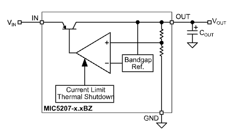
Low-Noise Fixed Regulator (TO-92 version only)
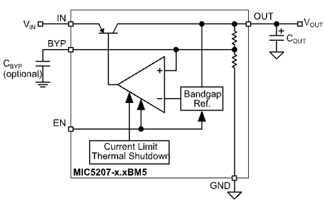
Ultra-Low-Noise Fixed Regulator
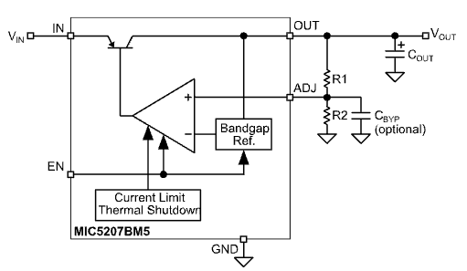
Ultra-Low-Noise Adjustable Regulator
Application Information
Enable/Shutdown
Driving the EN (enable/shutdown) pin high (> 2V) activates the regulator. The EN pin is fully compatible with CMOS logic levels.
If the enable/shutdown function is not needed, simply tie EN (pin 3) to IN (supply input, pin 1). See Figure 1.
Input Capacitor
A 1μF capacitor should be connected between IN and GND whenever the input source is more than 10 inches away from the AC filter capacitor, or when the regulator is powered by a battery.
Reference Bypass Capacitor (BYP)
The BYP pin is tied to the internal voltage reference. Adding a 470pF capacitor (CBYP) between BYP and GND helps suppress noise, greatly lowering output noise levels.
However, CBYP also reduces phase margin. To maintain stability when CBYP is used, output capacitors of 2.2μF or greater are recommended.
The MIC5207’s startup time is inversely related to the value of CBYP:
- Larger CBYP → slower ramp-up of output voltage (useful if a gradual startup is desired).
- Smaller CBYP or none → faster startup (preferred if quick turn-on is required).
If output noise performance is not critical, CBYP can be omitted, and the BYP pin may be left open.
Output Capacitor
An output capacitor must be placed between OUT and GND to ensure stability and prevent oscillation. The required minimum capacitance depends on whether a reference bypass capacitor (CBYP) is used:
- Without CBYP: At least 1.0μF (see Figure 2).
- With 470pF CBYP: At least 2.2μF (see Figure 1).
Using larger capacitors further improves transient response, and there is no upper limit to the output capacitance.
For reliable operation, the output capacitor should have an ESR of 5Ω or less and a resonant frequency above 1MHz. Extremely low-ESR capacitors may cause low-level oscillations or underdamped transient response.
- Tantalum or aluminum electrolytic capacitors are generally suitable.
- Film capacitors are also effective but typically more costly.
- Since many aluminum electrolytics freeze around –30°C, solid tantalum capacitors are preferred for applications below –25°C.
At low output currents, the capacitance requirement decreases:
- 0.47μF is sufficient for currents below 10mA.
- 0.33μF is sufficient for currents below 1mA.
No-Load Stability
The MIC5207 remains stable and maintains regulation even with no load (except for the internal voltage divider), unlike many other voltage regulators. This feature is especially useful for CMOS RAM keep-alive applications.
Thermal Considerations
The MIC5207 is capable of providing 180mA continuous output in a very compact package. Maximum power dissipation depends on the voltage drop across the regulator and the output current.
The maximum power dissipation can be calculated using the device’s junction-to-ambient thermal resistance (θJA) and the equation:PD(MAX)=TJ(max)−TAθJAPD(MAX) = \frac{T_{J(max)} - T_A}{\theta_{JA}}PD(MAX)=θJATJ(max)−TA
Where:
- TJ(max)T_{J(max)}TJ(max) = maximum junction temperature (125°C)
- TAT_ATA = ambient operating temperature
- θJA = junction-to-ambient thermal resistance, layout-dependent (see Table 1).
Table 1. SOT-23-5 Thermal Resistance
| Package | θJA (Recommended Minimum Footprint) | θJA (1”² Copper Clad) | θJ/C |
|---|---|---|---|
| SOT-23-5 (M5) | 235°C/W | 170°C/W | 130°C/W |
The actual power dissipation of the regulator can be calculated as:PD=(VIN−VOUT)⋅IOUT+VIN⋅IGNDPD = (VIN - VOUT) \cdot IOUT + VIN \cdot IGNDPD=(VIN−VOUT)⋅IOUT+VIN⋅IGND
By substituting PD(MAX) for PD, you can determine the maximum operating conditions for the regulator in a specific application.
Example:
For a MIC5207-3.3BM5 at room temperature with a minimum footprint layout:PD(MAX)=125°C−25°C235°C/W=425 mWPD(MAX) = \frac{125°C - 25°C}{235°C/W} = 425\,\text{mW}PD(MAX)=235°C/W125°C−25°C=425mW
From Table 1, the junction-to-ambient thermal resistance for the minimum footprint is 220°C/W. Using an output voltage of 3.3V and an output current of 150mA:PD=(VIN−3.3V)⋅150 mA+(3 mA⋅VIN)PD = (VIN - 3.3V) \cdot 150\,\text{mA} + (3\,\text{mA} \cdot VIN)PD=(VIN−3.3V)⋅150mA+(3mA⋅VIN)
Solving:PD=455 mW+3 mA⋅VIN≤425 mWPD = 455\,\text{mW} + 3\,\text{mA} \cdot VIN \leq 425\,\text{mW}PD=455mW+3mA⋅VIN≤425mW
This calculation shows the maximum input voltage allowable for safe operation without exceeding thermal limits.
Low-Voltage Operation
Special care is required when using the MIC5207-1.8 and MIC5207-2.5 in voltage-sensitive systems, as their output may momentarily overshoot during startup unless proper output and bypass capacitor values are selected.
During power-up, the pass transistor saturates briefly while the error amplifier and voltage reference power up more slowly from the output (see “Block Diagram”). Using larger output and bypass capacitors allows extra time for the error amplifier and reference to stabilize, preventing overshoot.
Recommended capacitor values:
- Light loads (~100μA): 4.7μF output capacitor + 470pF bypass capacitor. This slows startup enough to prevent the output voltage from exceeding its nominal value.
- Heavier loads: 10μF output capacitor + 470pF bypass capacitor.
Smaller capacitors can be used depending on system sensitivity.
- If some overshoot is acceptable: Output and/or bypass capacitors can be reduced or eliminated.
- For systems tolerant of overshoot due to power-on reset delays: Standard output and bypass capacitor values may be used.
Note: The junction temperature range for 1.8V versions (fixed or adjustable) is 0°C to +125°C.
For a 3.3V application with 150mA output current, the maximum allowable input voltage in a SOT-23-5 package is 6V. For a detailed discussion of heat sinking and thermal considerations for voltage regulators, see the “Regulator Thermals” section in Micrel’s Designing with Low-Dropout Voltage Regulators handbook.
Fixed Regulator Applications
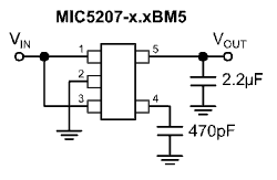
Figure 1 Ultra-Low-Noise Fixed Voltage Application
Figure 1 shows an example circuit for ultra-low-noise operation:
- A 470pF capacitor is connected to BYP for noise reduction.
- EN (pin 3) is tied to IN (pin 1) for applications where the enable/shutdown function is not needed.
- The output capacitor (COUT) should be at least 2.2μF.
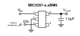
Figure 2 Low-Noise Fixed Voltage Application
Figure 2 shows a basic low-noise configuration, with a minimum COUT = 1μF.
Adjustable Regulator Applications
The MIC5207BM5 can be set to a specific output voltage using two external resistors (Figure 3). The output voltage is determined by:VOUT=VREF(1+R1R2)+IADJ⋅R1V_{OUT} = V_{REF} \left( 1 + \frac{R1}{R2} \right) + I_{ADJ} \cdot R1VOUT=VREF(1+R2R1)+IADJ⋅R1
Where VREF = 1.242V.
- This equation works because the bandgap reference is relative to the output, unlike traditional regulators where the reference is relative to ground.
- Resistor values are not critical due to the high input impedance of the ADJ pin, but using 470kΩ or less is recommended for best results.
- Adding a capacitor from ADJ to GND significantly reduces output noise.
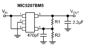
Figure 3 Ultra-Low-Noise Adjustable Voltage Application
Figure 3 shows an ultra-low-noise adjustable voltage application, including the optional 470pF bypass capacitor from ADJ to GND.
Dual-Supply Operation
When operating in dual-supply systems (with the load returned to a negative supply), the output voltage must be diode-clamped to ground.
USB Application
Figure 4 illustrates the MIC5207-3.3BZ (3-terminal, TO-92) used in a USB application. Since the VBUS supply may be more than 10 inches from the regulator, a 1μF input capacitor is included to maintain stability.
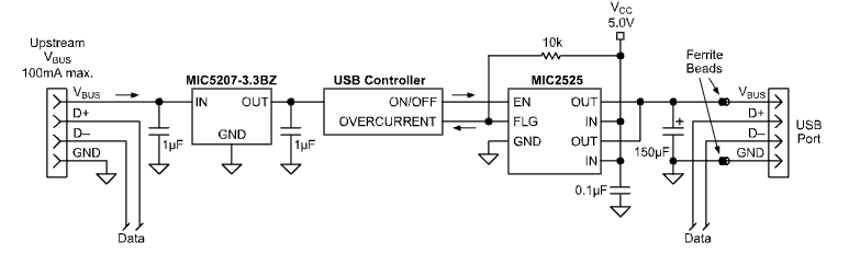
Figure 4. Single-Port Self-Powered Hub
Package Information
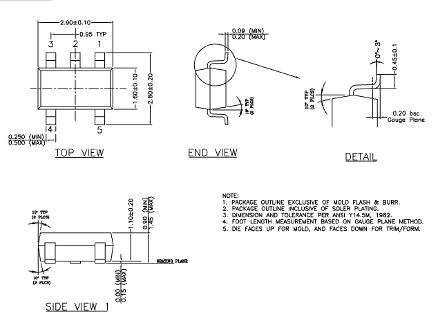
5-Pin SOT-23 (M5)
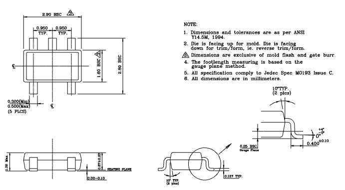
5-Pin Thin SOT-23 (D5)
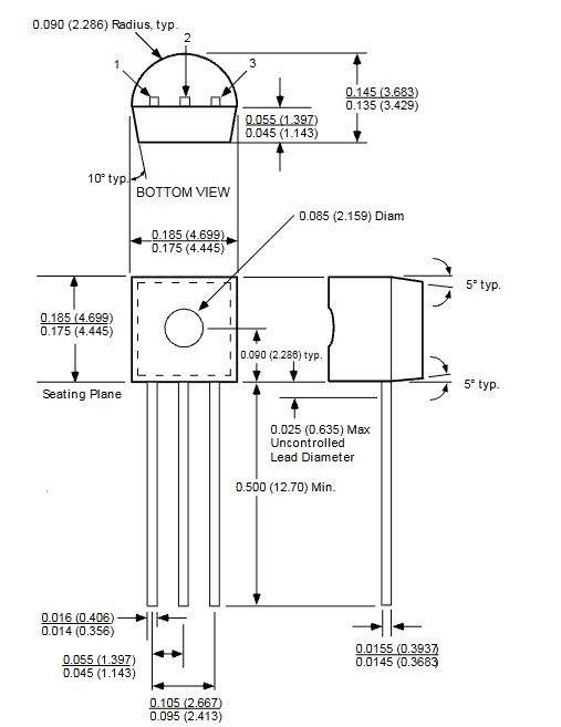
3-Pin TO-92 (Z)
Conclusion
The MIC5207 is a versatile, ultra-low-noise LDO regulator suitable for a wide range of applications, including battery-powered and USB devices. Its low dropout voltage, high output accuracy, and flexible enable/shutdown feature make it ideal for sensitive systems. Proper selection of output and bypass capacitors ensures stability, low noise, and controlled startup, while adjustable versions allow precise voltage settings. Thermal considerations and low-voltage operation guidelines help optimize performance and reliability in compact designs.

Christopher Anderson
Christopher Anderson has a Ph.D. in electrical engineering, focusing on power electronics. He’s been a Senior member of the IEEE Power Electronics Society since 2021. Right now, he works with the KPR Institute of Engineering and Technology in the U.S. He also writes detailed, top-notch articles about power electronics for business-to-business electronics platforms.
Subscribe to JMBom Electronics !


