


TL431/TL432 Applications Overview
Catalog
DescriptionOverviewFeatures Device Functional ModesApplicationsDevice InformationApplications and ImplementationPin Configuration and FunctionsSpecificationsElectrical Characteristics – TL431C, TL432CElectrical Characteristics – TL431I, TL432IElectrical Characteristics – TL431Q, TL432Q Typical ApplicationsConclusionDescription
The TL431 and TL432 are three-terminal adjustable shunt regulators designed with specified thermal stability across automotive, commercial, and military temperature ranges. By using two external resistors, the output voltage can be adjusted anywhere between the reference voltage (about 2.5 V) and 36 V. These regulators feature a typical output impedance of 0.2 Ω.
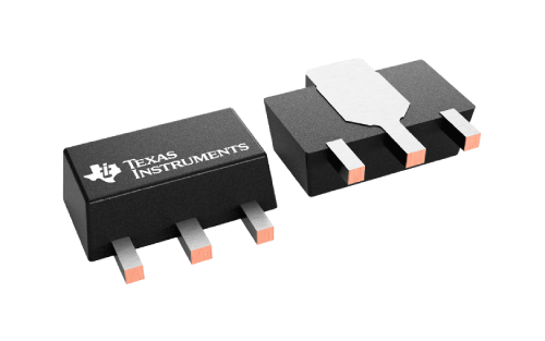
TL431 and TL432
Thanks to their active output circuitry, they deliver a sharp turn-on response, making them excellent alternatives to Zener diodes in applications like on-board regulation, adjustable power supplies, and switching power supplies. Functionally and electrically, the TL432 is identical to the TL431, except for the pin configurations in the DBV, DBZ, and PK packages.
Both TL431 and TL432 are available in three precision grades, with initial tolerances (at 25°C) of 0.5% (B grade), 1% (A grade), and 2% (standard grade). Additionally, low output drift with temperature ensures reliable stability across the full temperature range.
For operating conditions:
- TL43xxC devices are rated from 0°C to 70°C
- TL43xxI devices are rated from –40°C to 85°C
- TL43xxQ devices are rated from –40°C to 125°C
Overview
The TL43xx family is one of those “go-to” analog parts you’ll find almost everywhere. Why? Because inside, it combines two super useful building blocks:
- a precision voltage reference, and
- a little op-amp.
With just these two things, you can make the chip act like:
- a voltage reference,
- an error amplifier,
- a voltage clamp, or even
- a comparator (with its own reference built in).
That’s why it shows up in everything from power supplies to signal conditioning circuits.
The TL43xx works across a wide voltage range — you can adjust its cathode voltage anywhere between 2.5 V and 36 V, which makes it flexible for industrial, automotive, telecom, or computing gear. But there’s one key rule: the cathode pin needs at least 1 mA (the minimum current) to actually regulate. Once that’s in place, you can feed some of the output back to the reference pin, and the chip basically “clones” its internal 2.5 V reference for your circuit.
You can also choose how precise you want your reference to be:
- B version → 0.5% tolerance
- A version → 1.0% tolerance
- Standard (no suffix) → 2.0% tolerance
And, to make life easier, there are two pinout options: TL431 and TL432. Functionally they’re the same, just arranged differently.
For temperature ratings, it comes in three “flavors”:
- C grade: 0°C to +70°C (commercial)
- I grade: –40°C to +85°C (industrial)
- Q grade: –40°C to +125°C (automotive/extended)
Features
- Reference voltage tolerance at 25°C: 0.5% (B grade) 1% (A grade) 2% (Standard grade)
- Adjustable output voltage from Vref up to 36 V
- Wide operating temperature range: –40°C to 125°C
- Typical temperature drift (TL43xB): 6 mV (C grade) 14 mV (I and Q grades)
- Low output noise
- Typical output impedance: 0.2 Ω
- Sink current range: 1 mA to 100 mA
Feature Description
Inside the TL43xx, you’ve basically got two things working together:
- a precision reference, and
- an amplifier.
What happens is: the chip compares the voltage at the REF pin with its internal reference. Based on that difference, it controls how much current it sinks (pulls down) through the cathode. This sink current is handled by an internal Darlington pair (two transistors back-to-back), which lets the device sink up to 100 mA — pretty beefy for a small IC.
Here’s how it behaves:
- As long as you give it enough voltage headroom (≥ 2.5 V) and enough cathode current (IKA), the TL431 will force the REF pin to sit at 2.5 V.
- BUT — you can’t just leave the REF pin hanging in the air. It needs a small current (at least 4 µA) to bias its internal transistor properly.
When you connect feedback between the cathode and the REF pin, the TL43xx starts acting a lot like a Zener diode, regulating to a stable voltage. The internal op-amp + reference keep things in the right operating region, and the gain is high enough for stable regulation.
Unlike most linear regulators, the TL431 is already internally compensated. That means it’s stable even without an output capacitor across cathode and anode. But — if you do want to use a capacitor for filtering or stability reasons, there’s guidance (Figure 6-18 in the datasheet) for picking the right one.
Device Functional Modes
Open Loop (Comparator Mode)
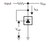
If you don’t feed the cathode/output back into the REF pin, then the device is in open-loop mode. With the right cathode current supplied, the TL431 basically acts like a comparator with a built-in 2.5 V reference. Because of its high gain, it can easily detect when an input signal crosses that threshold. This makes it handy for things like voltage monitoring or simple threshold detection.
Closed Loop (Shunt Regulator Mode)
If you do feed back the output voltage (from cathode) to the REF pin, then it’s in closed-loop mode. This is the most common way people use the TL431. In this configuration, it works like an error amplifier that continuously adjusts itself to keep the output voltage steady.
Basically:
- Part of the output voltage is fed back to REF (using resistors or direct wiring).
- The device compares it to the internal 2.5 V reference.
- It then sinks just the right amount of current to keep the output regulated.
That’s why you’ll often see TL431s in power supplies, chargers, and regulators — they’re simple, accurate, and flexible.
Applications
- Rack server power systems
- Industrial AC/DC supplies
- AC inverters and variable frequency drives
- Servo drive control modules
- Notebook PC power adapter designs
Simplified Schematic
Device Information
| Part Number | Package (Pin Count)¹ | Body Size (Nominal)² |
|---|---|---|
| TL43x | SOT-23-3 (3) | 2.90 mm × 1.30 mm |
| TL43x | SOT-23-5 (5) | 2.90 mm × 1.60 mm |
| TL43x | SOIC (8) | 4.90 mm × 3.90 mm |
| TL43x | PDIP (8) | 9.50 mm × 6.35 mm |
| TL43x | SOP (8) | 6.20 mm × 5.30 mm |
¹ For a full list of available packages, refer to the orderable addendum at the end of this datasheet.
² Package size (length × width) represents nominal values and includes pins where applicable.
Applications and Implementation
Quick heads-up first:
The stuff in this section isn’t part of the official TI specs. It’s more like guidance and ideas. TI can’t guarantee every single use case, so it’s up to the designer (yep, that’s you) to test and validate the circuit in your system. Think of it like: TI gives you the building blocks, but you’ve got to make sure the whole house stands up in your own backyard.
Application Information
The TL431/TL432 are super flexible, and because of that, there’s no way the datasheet can cover every single possible setup. Different loads, capacitors, and feedback networks can all affect how the device behaves.
To help out, TI points you to a couple of really useful application notes:
- SLVA482 – “Understanding Stability Boundary Conditions Charts in TL431, TL432 Data Sheet” → This one digs deep into stability. It explains how to read those stability charts, and how to pick the right capacitor if you want to keep the TL431 behaving nicely in your design.
- SLVA445 – “Setting the Shunt Voltage on an Adjustable Shunt Regulator” → This one’s more about the practical setup. It walks you through how to properly set the shunt voltage when you’re using the TL431/TL432 as an adjustable regulator.
In short: these notes are like extra “cheat sheets” that make designing with TL431 easier and way less guesswork.
Pin Configuration and Functions
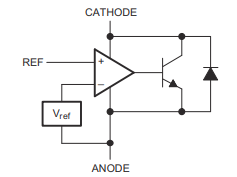
Equivalent Schematic
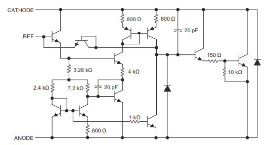
Detailed Schematic
Specifications
Absolute Maximum Ratings
(Over operating free-air temperature range, unless otherwise noted)¹
| Parameter | Min | Max | Unit |
|---|---|---|---|
| VKA – Cathode Voltage² | — | 37 | V |
| IKA – Continuous Cathode Current | –100 | 150 | mA |
| II(ref) – Reference Input Current | –0.05 | 10 | mA |
| TJ – Operating Junction Temperature | — | 150 | °C |
| Tstg – Storage Temperature | –65 | 150 | °C |
¹ Stresses beyond these limits may cause permanent damage. These ratings define stress conditions only and do not guarantee device functionality under such conditions. Continuous exposure to maximum ratings may affect long-term reliability.
² All voltages are referenced to the anode, unless otherwise specified.
ESD Ratings
| Model | Value | Unit |
|---|---|---|
| Human Body Model (HBM), ANSI/ESDA/JEDEC JS-001¹ | ±2000 | V |
| Charged Device Model (CDM), JEDEC JESD22-C101² | ±1000 | V |
¹ Per JEDEC JEP155, 500 V HBM is considered safe for standard ESD-controlled manufacturing. Lower ratings require stricter precautions.
² Per JEDEC JEP157, 250 V CDM is considered safe for standard ESD-controlled manufacturing. Lower ratings require stricter precautions.
Thermal Information
| Thermal Metric¹ | Package (Pins) | Value (°C/W) |
|---|---|---|
| RθJA – Junction-to-ambient | P (8) | 85 |
| PW (6) | 149 | |
| D (8) | 97 | |
| PS (8) | 95 | |
| DCK (3) | 259 | |
| DBV (5) | 206 | |
| DBZ (5) | 206 | |
| LP (8) | 140 | |
| PK (8) | 52 | |
| RθJC(top) – Junction-to-case (top) | P (8) | 57 |
| PW (6) | 65 | |
| D (8) | 39 | |
| PS (8) | 46 | |
| DCK (3) | 87 | |
| DBV (5) | 131 | |
| DBZ (5) | 76 | |
| LP (8) | 55 | |
| PK (8) | 9 |
¹ For details on standard and new thermal metrics, refer to IC Package Thermal Metrics application report (SPRA953).
Recommended Operating Conditions
| Parameter | Min | Max | Unit |
|---|---|---|---|
| VKA – Cathode Voltage | Vref | 36 | V |
| IKA – Continuous Cathode Current | 1 | 100 | mA |
| TA – Free-Air Operating Temperature | °C | ||
| • TL43xxC | 0 | 70 | |
| • TL43xxI | –40 | 85 | |
| • TL43xxQ | –40 | 125 |
¹ Maximum power dissipation depends on TJ(max), θJA, and TA. The allowable dissipation is:PD=TJ(max)–TAθJAP_D = \frac{T_J(max) – T_A}{θ_{JA}}PD=θJATJ(max)–TA
Operating at the absolute maximum TJ of 150°C may reduce device reliability.
Electrical Characteristics – TL431C, TL432C
(Over recommended operating conditions, TA = 25°C unless otherwise noted)
| Parameter | Test Circuit | Test Conditions | Min | Typ | Max | Unit |
|---|---|---|---|---|---|---|
| Vref – Reference Voltage | Fig. 7-1 | VKA = Vref, IKA = 10 mA | 2440 | 2495 | 2550 | mV |
| VI(dev) – Deviation of Reference Input Voltage over Full Temperature Range¹ | Fig. 7-1 | VKA = Vref, IKA = 10 mA SOT-23-3 and TL432 devices | 6 | — | 16 | mV |
| All other devices | 4 | — | 25 | mV | ||
| ΔVref / ΔVKA – Ratio of Change in Reference Voltage to Change in Cathode Voltage | Fig. 7-2 | IKA = 10 mA ΔVKA = 10 V – Vref | –1 | — | –2.7 | mV/V |
| ΔVKA = 36 V – 10 V | –1 | — | –2 | mV/V | ||
| Iref – Reference Input Current | Fig. 7-2 | IKA = 10 mA, R1 = 10 kΩ, R2 = ∞ | 2 | — | 4 | µA |
| II(dev) – Deviation of Reference Input Current over Full Temperature Range¹ | Fig. 7-2 | IKA = 10 mA, R1 = 10 kΩ, R2 = ∞ | 0.4 | — | 1.2 | µA |
| Imin – Minimum Cathode Current for Regulation | Fig. 7-1 | VKA = Vref | 0.4 | — | 1 | mA |
| Ioff – Off-State Cathode Current | Fig. 7-3 | VKA = 36 V, Vref = 0 | 0.1 | — | 1 | µA |
| ZKA | – Dynamic Impedance² | Fig. 7-1 | VKA = Vref, f ≤ 1 kHz, IKA = 1 mA to 100 mA | 0.2 | — |
¹ The deviation parameters VI(dev) and II(dev) are defined as the difference between the maximum and minimum values measured across the rated temperature range. For more details on VI(dev) and its relationship to the average temperature coefficient, see Temperature Coefficient.
² The dynamic impedance is given by:∣ZKA∣=ΔVKAΔIKA|Z_{KA}| = \frac{ΔV_{KA}}{ΔI_{KA}}∣ZKA∣=ΔIKAΔVKA
For more information on how |ZKA| relates to VKA, see Dynamic Impedance.
Electrical Characteristics – TL431I, TL432I
(Over recommended operating conditions, TA = 25°C unless otherwise noted)
| Parameter | Test Circuit | Test Conditions | Min | Typ | Max | Unit |
|---|---|---|---|---|---|---|
| Vref – Reference Voltage | Fig. 7-1 | VKA = Vref, IKA = 10 mA | 2440 | 2495 | 2550 | mV |
| VI(dev) – Deviation of Reference Input Voltage over Full Temperature Range¹ | Fig. 7-1 | VKA = Vref, IKA = 10 mA SOT-23-3 and TL432 devices | 14 | — | 34 | mV |
| All other devices | 5 | — | 50 | mV | ||
| ΔVref / ΔVKA – Ratio of Change in Reference Voltage to Change in Cathode Voltage | Fig. 7-2 | IKA = 10 mA ΔVKA = 10 V – Vref | –1.4 | — | –2.7 | mV/V |
| ΔVKA = 36 V – 10 V | –1 | — | –2 | mV/V | ||
| Iref – Reference Input Current | Fig. 7-2 | IKA = 10 mA, R1 = 10 kΩ, R2 = ∞ | 2 | — | 4 | µA |
| II(dev) – Deviation of Reference Input Current over Full Temperature Range¹ | Fig. 7-2 | IKA = 10 mA, R1 = 10 kΩ, R2 = ∞ | 0.8 | — | 2.5 | µA |
| Imin – Minimum Cathode Current for Regulation | Fig. 7-1 | VKA = Vref | 0.4 | — | 1 | mA |
| Ioff – Off-State Cathode Current | Fig. 7-3 | VKA = 36 V, Vref = 0 | 0.1 | — | 1 | µA |
| ZKA | – Dynamic Impedance² | Fig. 7-1 | VKA = Vref, f ≤ 1 kHz, IKA = 1 mA to 100 mA | 0.2 | — |
¹ The deviation parameters VI(dev) and II(dev) are defined as the difference between the maximum and minimum values measured across the rated temperature range. For details on VI(dev) and its relationship to the average temperature coefficient, see Temperature Coefficient.
² The dynamic impedance is calculated as:∣ZKA∣=ΔVKAΔIKA|Z_{KA}| = \frac{ΔV_{KA}}{ΔI_{KA}}∣ZKA∣=ΔIKAΔVKA
Electrical Characteristics – TL431Q, TL432Q
(Over recommended operating conditions, TA = 25°C unless otherwise noted)
| Parameter | Test Circuit | Test Conditions | Min | Typ | Max | Unit |
|---|---|---|---|---|---|---|
| Vref – Reference Voltage | Fig. 7-1 | VKA = Vref, IKA = 10 mA | 2440 | 2495 | 2550 | mV |
| VI(dev) – Deviation of Reference Input Voltage over Full Temperature Range¹ | Fig. 7-1 | VKA = Vref, IKA = 10 mA | 14 | — | 34 | mV |
| ΔVref / ΔVKA – Ratio of Change in Reference Voltage to Change in Cathode Voltage | Fig. 7-2 | IKA = 10 mA ΔVKA = 10 V – Vref | –1.4 | — | –2.7 | mV/V |
| ΔVKA = 36 V – 10 V | –1 | — | –2 | mV/V | ||
| Iref – Reference Input Current | Fig. 7-2 | IKA = 10 mA, R1 = 10 kΩ, R2 = ∞ | 2 | — | 4 | µA |
| II(dev) – Deviation of Reference Input Current over Full Temperature Range¹ | Fig. 7-2 | IKA = 10 mA, R1 = 10 kΩ, R2 = ∞ | 0.8 | — | 2.5 | µA |
| Imin – Minimum Cathode Current for Regulation | Fig. 7-1 | VKA = Vref | 0.4 | — | 1 | mA |
| Ioff – Off-State Cathode Current | Fig. 7-3 | VKA = 36 V, Vref = 0 | 0.1 | — | 1 | µA |
| ZKA | – Dynamic Impedance² | Fig. 7-1 | VKA = Vref, f ≤ 1 kHz, IKA = 1 mA to 100 mA | 0.2 | — |
¹ The deviation parameters VI(dev) and II(dev) are defined as the difference between the maximum and minimum values measured across the rated temperature range. For details on VI(dev) and its relationship to the average temperature coefficient, see Temperature Coefficient.
² The dynamic impedance is calculated as:∣ZKA∣=ΔVKAΔIKA|Z_{KA}| = \frac{ΔV_{KA}}{ΔI_{KA}}∣ZKA∣=ΔIKAΔVKA
For more information on how |ZKA| varies with VKA, see Dynamic Impedance.
Typical Applications
Comparator With Integrated Reference
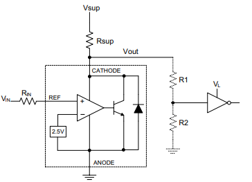
Comparator Application Schematic
Conclusion
The TL431/TL432 are highly versatile adjustable shunt regulators suitable for a wide range of applications. Designers must validate their specific implementations, and TI’s application notes provide guidance on stability, capacitor selection, and setting the shunt voltage to ensure reliable and accurate operation.

Christopher Anderson
Christopher Anderson has a Ph.D. in electrical engineering, focusing on power electronics. He’s been a Senior member of the IEEE Power Electronics Society since 2021. Right now, he works with the KPR Institute of Engineering and Technology in the U.S. He also writes detailed, top-notch articles about power electronics for business-to-business electronics platforms.
Subscribe to JMBom Electronics !


