


TL43xx Regulators Design Summary
Catalog
Description Overview Functional Block DiagramFeature DescriptionDevice Functional ModesApplications and Implementation Typical ApplicationsDesign Requirements Application CurvePin Configuration and FunctionsParameter Measurement InformationDynamic ImpedanceConclusionDescription
The TL431 and TL432 are three-terminal adjustable shunt regulators designed with reliable thermal stability across automotive, commercial, and military temperature ranges. By using just two external resistors, the output voltage can be set anywhere from Vref (around 2.5V) up to 36V. These devices feature a typical output impedance of 0.2Ω.
TL43xx Regulators
With their sharp turn-on characteristics, thanks to the active output circuitry, they serve as excellent alternatives to Zener diodes in a wide range of applications, including on-board regulation, adjustable power supplies, and switching power supplies.
The TL432 shares the same functionality and electrical performance as the TL431 but comes with different pin configurations in the DBV, DBZ, and PK packages. Both devices are available in three precision grades, offering initial tolerances at 25°C of 0.5% (B grade), 1% (A grade), and 2% (standard grade). In addition, low temperature-related output drift ensures stable performance across the entire temperature range.
Operating ranges are defined as follows: TL43xxC devices work from 0°C to 70°C, TL43xxI devices from –40°C to 85°C, and TL43xxQ devices from –40°C to 125°C.
Overview
The TL43xx series is a widely used and versatile device, suitable for applications ranging from power management to signal processing. Its versatility comes from its two core building blocks—an accurate voltage reference and an operational amplifier—both of which are fundamental in analog design.
By combining these key elements, the TL43xx can function as a precision voltage reference, error amplifier, voltage clamp, or comparator with an integrated reference. The device supports adjustable cathode voltages from 2.5 V to 36 V, making it an excellent choice for industrial, automotive, telecom, and computing applications.
For proper operation as a shunt regulator or error amplifier, the cathode pin must be supplied with at least 1 mA (Imin(max)). When this condition is met, feedback between the Cathode and Reference pins can replicate the internal reference voltage.
Devices are available with different reference voltage accuracy options, specified at 25°C:
- B grade: 0.5%
- A grade: 1%
- Standard grade: 2%
The TL431 and TL432 provide the same functionality, but with different pinout configurations to fit various package options.
Temperature ranges are as follows:
- TL43xxC: 0°C to 70°C
- TL43xxI: –40°C to 85°C
- TL43xxQ: –40°C to 125°C
Functional Block Diagram
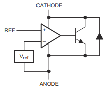
Equivalent Schematic
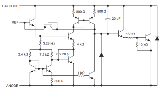
Detailed Schematic
Feature Description
The TL43xx series combines an internal voltage reference and amplifier that generate a sink current based on the difference between the reference pin and the internal virtual reference. This sink current is delivered through an internal Darlington pair (see Figure 8-2), which allows the device to handle up to 100 mA.
When supplied with sufficient voltage headroom (≥ 2.5 V) and cathode current (IKA), the TL431 maintains the reference pin at 2.5 V. The reference pin, however, must not be left floating; it requires a minimum current of IREF ≥ 4 µA (see Electrical Characteristics for TL431C/TL432C). This is necessary because the reference pin drives an internal NPN transistor, which requires base current to operate correctly.
With feedback applied from the Cathode to the Reference pin, the TL43xx behaves like a Zener diode, regulating at a constant voltage determined by the current supplied into the cathode. This regulation occurs because the internal amplifier and reference enter their correct operating regions. For proper linear operation and sufficient gain, the same minimum current must also be applied when the device is used in open-loop, servo, or error-amplifier applications.
Unlike many traditional linear regulators, the TL43xx is internally compensated and does not require an output capacitor between the cathode and anode for stability. However, if an external capacitor is desired, Figure 6-18 provides guidance for selecting an appropriate value to ensure stable operation.
Device Functional Modes
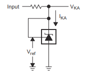
Open Loop (Comparator Mode)
When the cathode/output voltage or current is not fed back to the reference/input pin, the TL43xx operates in open loop. With sufficient cathode current (IKA), the device exhibits the characteristics shown in Figure 9-2. In this configuration, its high gain allows it to be used as a comparator. Because the reference is built-in, the TL43xx is a preferred choice for monitoring a single signal against a defined threshold.
Closed Loop (Regulation Mode)
When the cathode/output voltage or current is fed back to the reference/input pin, the TL43xx operates in closed loop. Most applications use the device in this mode to regulate a fixed voltage or current. The feedback allows the TL43xx to function as an error amplifier, sampling a portion of the output and adjusting it to maintain regulation. This is achieved by driving the reference pin to match the internal 2.5 V reference, which can be done through resistive or direct feedback.
Applications and Implementation
Note:
The application information in this section is provided as guidance only and is not part of the TI component specification. TI does not guarantee its accuracy or completeness. Customers are responsible for evaluating whether this device is suitable for their application and must validate and test their designs to confirm proper functionality.
Application Information
Because the TL43xx can be used in a wide variety of circuits and configurations, it is not possible for this datasheet to cover every scenario in detail. For additional design guidance, the following application notes are recommended:
- Understanding Stability Boundary Conditions Charts in TL431, TL432 Data Sheet (SLVA482): Explains the device’s stability characteristics and helps designers select appropriate load capacitors.
- Setting the Shunt Voltage on an Adjustable Shunt Regulator (SLVA445): Provides methods for accurately setting the shunt voltage to achieve the best possible precision.
Typical Applications
Comparator with Integrated Reference
(Details would follow in the datasheet application circuit description.)
Comparator Application Schematic
Design Requirements
For this design example, use the input parameters listed in Table.
Table Design Parameters
| Design Parameter | Example Value |
|---|---|
| Input Voltage Range | 0 V to 5 V |
| Input Resistance | 10 kΩ |
| Supply Voltage | 24 V |
| Cathode Current (IK) | 5 mA |
| Output Voltage Level | ~2 V – VSUP |
| Logic Input Thresholds (VIH / VIL) | VL |
Detailed Design Procedure
When using the TL431 as a comparator with integrated reference, determine the following design considerations:
- Input voltage range
- Reference voltage accuracy
- Logic input high and low level thresholds
- Current source resistance
Basic Operation
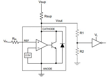
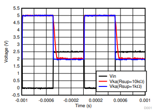
In the configuration shown in Figure 9-1, the TL431 operates as a comparator, comparing the voltage at the VREF pin to the internal virtual reference voltage. When supplied with sufficient cathode current (IK), the TL43xx provides high open-loop gain for fast response.
Figure 9-2 illustrates the effect of cathode current on response speed: with RSUP = 10 kΩ (IKA = 500 µA), the response is slower than with RSUP = 1 kΩ (IKA = 5 mA). Operating near or below the minimum current (Imin) reduces gain, resulting in slower response times.
Overdrive Considerations
Slow or inaccurate responses can also occur if the reference pin is not provided sufficient overdrive voltage—the amount above the internal virtual reference. The internal virtual reference is nominally 2.5 V, with tolerance depending on the device version (±0.5%, ±1.0%, or ±1.5%). Providing more overdrive voltage improves response speed.
For comparator applications, it is recommended to set the trip point above the expected positive error (e.g., +1% for the A version). For fast response, setting the trip point to more than 10% above the internal VREF is generally sufficient.
To minimize voltage drop or difference between Vin and the reference pin, use an input resistor below 10 kΩ to ensure adequate IREF.
Output Voltage and Logic Input Level
For proper operation of the TL431 as a comparator, its output must be compatible with the logic levels of the receiving device. This requires understanding the high and low input voltage thresholds, typically denoted VIH (input high) and VIL (input low).
In open-loop/comparator mode, the TL431’s output low voltage is approximately 2 V (Figure 9-2), which is generally sufficient for 5 V logic systems. However, this voltage may be too high for 3.3 V or 1.8 V logic. To address this, a resistive voltage divider can be used at the output to scale the voltage to levels readable by lower-voltage logic devices.
The TL431’s output high voltage equals VSUP, since it is an open-collector device. If VSUP exceeds the maximum input voltage tolerated by the receiving logic, the output should also be attenuated with a resistive divider to ensure reliable operation.
When using a resistive divider (R1 & R2 in Figure 9-1), ensure that the total resistance is significantly higher than RSUP. This prevents the divider from interfering with the TL431’s ability to pull the output close to VSUP when turning off.
Input Resistance
The TL431 requires an input resistor to provide the reference current (IREF) necessary to operate correctly in the active region. The voltage at the reference pin is given by:VREF=VIN−IREF⋅RINV_{REF} = V_{IN} - I_{REF} \cdot R_{IN}VREF=VIN−IREF⋅RIN
Since IREF can be up to 4 µA, it is recommended to use a sufficiently low input resistance to minimize the voltage drop and associated error, ensuring accurate operation.
Application Curve
Output Response With Various Cathode Currents
Shunt Regulator/Reference
Design Requirements
For this design example, use the input parameters listed in Table .
Table Design Parameters
| Design Parameter | Example Value |
|---|---|
| Reference Initial Accuracy | 1.0% |
| Supply Voltage | 24 V |
| Cathode Current (IK) | 5 mA |
| Output Voltage Level | 2.5 V – 36 V |
| Load Capacitance | 10 μF |
| Feedback Resistor Values & Accuracy (R1 & R2) | 10 kΩ |
Detailed Design Procedure
When using the TL431 as a shunt regulator, determine the following design considerations:
- Input voltage range
- Temperature range
- Total accuracy
- Cathode current
- Reference initial accuracy
- Output capacitance
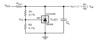
Programming the Output/Cathode Voltage
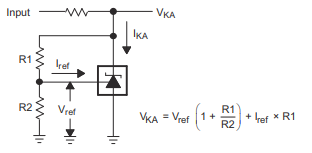
To set the cathode to a regulated voltage, a resistive bridge must be connected between the cathode and anode pins, with the midpoint tied to the reference pin (see Figure 9-3). The resistors R1 and R2 form this bridge.
The cathode/output voltage in this shunt regulator configuration can be approximated by:VO=(1+R1R2)⋅VREF−IREF⋅R1V_O = \left(1 + \frac{R1}{R2}\right) \cdot V_{REF} - I_{REF} \cdot R1VO=(1+R2R1)⋅VREF−IREF⋅R1
This formula accounts for the effect of reference current (IREF).
For accurate regulation, the TL43xx must be fully biased with sufficient open-loop gain to minimize gain error. This is achieved by supplying a cathode current at or above the minimum value specified in the Electrical Characteristics for TL431C/TL432C (Imin).
Device Information
Part Number: TL43x
Available Packages (Pin Count) and Body Size (Nominal):
- SOT-23-3 (3 pins): 2.90 mm × 1.30 mm
- SOT-23-5 (5 pins): 2.90 mm × 1.60 mm
- SOIC (8 pins): 4.90 mm × 3.90 mm
- PDIP (8 pins): 9.50 mm × 6.35 mm
- SOP (8 pins): 6.20 mm × 5.30 mm
(1) For a complete list of available packages, see the orderable addendum at the end of this data sheet.
(2) Body size values (length × width) are nominal and include pins where applicable.
Features
- Precision reference voltage tolerance at 25°C: • 0.5% (B grade) • 1% (A grade) • 2% (Standard grade)
- Adjustable output voltage from Vref (≈2.5 V) up to 36 V
- Wide operating temperature range: −40°C to 125°C
- Typical temperature drift (TL43xB): • 6 mV (Commercial temp) • 14 mV (Industrial & Automotive temp)
- Low output noise
- Typical output impedance: 0.2 Ω
- Sink current range: 1 mA to 100 mA
Applications
- Rack server power supplies
- Industrial AC/DC power systems
- AC inverters and variable-frequency drives
- Servo drive control modules
- Notebook PC power adapters
Pin Configuration and Functions
Specifications
Absolute Maximum Ratings
(over operating free-air temperature range, unless otherwise noted)
| Parameter | Min | Max | Unit |
|---|---|---|---|
| VKA – Cathode Voltage(2) | – | 37 | V |
| IKA – Continuous Cathode Current Range | –100 | 150 | mA |
| II(ref) – Reference Input Current | –0.05 | 10 | mA |
| TJ – Operating Junction Temperature | – | 150 | °C |
| Tstg – Storage Temperature Range | –65 | 150 | °C |
(1) Exceeding these absolute maximum ratings may cause permanent damage. Functional operation at or beyond these limits is not guaranteed. Prolonged exposure may affect long-term reliability.
(2) All voltages are referenced to ANODE unless otherwise specified.
ESD Ratings
| Model | Value | Unit |
|---|---|---|
| Human Body Model (HBM), ANSI/ESDA/JEDEC JS-001 (1) | ±2000 | V |
| Charged Device Model (CDM), JEDEC JESD22-C101 (2) | ±1000 | V |
(1) Per JEDEC JEP155, 500V HBM is considered safe for standard ESD handling. Lower levels require extra precautions.
(2) Per JEDEC JEP157, 250V CDM is considered safe for standard ESD handling. Lower levels require extra precautions.
Thermal Information
| Thermal Metric(1) | TL43xx | Unit |
|---|---|---|
| Junction-to-ambient thermal resistance (RθJA) | 85 (P, 8 pins), 149 (PW, 6 pins), 97 (D, 8 pins), 95 (PS, 8 pins), 259 (DCK, 3 pins), 206 (DBV, 5 pins), 206 (DBZ, 3 pins), 140 (LP), 52 (PK) | °C/W |
| Junction-to-case (top) thermal resistance (RθJC, top) | 57 (P), 65 (PW), 39 (D), 46 (PS), 87 (DCK), 131 (DBV), 76 (DBZ), 55 (LP), 9 (PK) | °C/W |
(1) For details on thermal metrics, see IC Package Thermal Metrics (application report SPRA953).
Recommended Operating Conditions
| Parameter | Min | Max | Unit |
|---|---|---|---|
| VKA – Cathode Voltage | Vref | 36 | V |
| IKA – Continuous Cathode Current Range | 1 | 100 | mA |
| TA – Operating Free-Air Temperature | °C | ||
| – TL43xxC | 0 | 70 | |
| – TL43xxI | –40 | 85 | |
| – TL43xxQ | –40 | 125 |
(1) Maximum power dissipation depends on TJ(max), θJA, and TA. It can be calculated as PD = (TJ(max) – TA)/θJA. Operating continuously at the maximum TJ of 150°C may reduce device reliability.
Parameter Measurement Information
Test Circuit for VKA = Vref
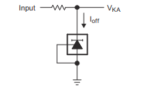
Test Circuit for Ioff
Temperature Coefficient
The variation of the reference voltage (Vref) across the full operating temperature range is referred to as VI(dev). This parameter can be used to calculate the device’s temperature coefficient. The average temperature coefficient of the reference input voltage over the full range, denoted as αVref, is defined as:
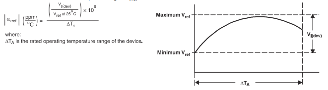
αVref can be either positive or negative, depending on whether the minimum Vref or maximum Vref occurs at the lower end of the temperature range. The full-range temperature coefficient is an average value, so within smaller portions of the rated operating temperature range, the coefficient may be higher or lower than the average. For additional information on temperature coefficients, see the Voltage Reference Selection Basics white paper.
Dynamic Impedance
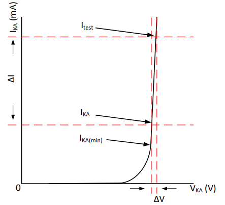
Dynamic impedance is defined as:ZKA=ΔVKAΔIKAZ_{KA} = \frac{ΔV_{KA}}{ΔI_{KA}}ZKA=ΔIKAΔVKA
When the device operates with two external resistors (see Figure 6-13), the total dynamic impedance of the circuit is:Z′=ΔVΔIZ' = \frac{ΔV}{ΔI}Z′=ΔIΔV
This can be approximated as:ZKA′≈R1R2⋅ZKAZ'_{KA} \approx \frac{R1}{R2} \cdot Z_{KA}ZKA′≈R2R1⋅ZKA
The cathode voltage (VKA) of the device can be influenced by dynamic impedance. The test current (Itest) used to specify VKA is listed in the Electrical Characteristics table. Any difference between the actual operating current and Itest may result in a shift in the output VKA. Figure 7-4 illustrates how dynamic impedance affects VKA.
Dynamic Impedance
Conclusion
The TL43xx series offers versatile functionality as both a comparator and a shunt regulator. By properly selecting input parameters, cathode current, feedback resistors, and considering reference accuracy, designers can achieve precise voltage regulation or fast comparator response. Correct implementation—including meeting minimum current requirements and accounting for IREF—ensures stable operation, reliable output voltage, and compatibility with the intended logic or load.

Amanda Miller
Amanda Miller is a senior electronics engineer with 6 years of experience. She focuses on studying resistors, transistors, and package design in detail. Her deep knowledge helps her bring innovation and high standards to the electronics industry.
Subscribe to JMBom Electronics !


