


What is a Complementary Metal Oxide Semiconductor (CMOS)?
Catalog
Introduction to MOS TechnologyCMOS (Complementary Metal-Oxide-Semiconductor)CMOS (Complementary Metal-Oxide-Semiconductor)CMOS Working PrincipleWhich Devices Use CMOS?CMOS InverterCMOS NAND GateCMOS NOR GateCMOS FabricationLifetime of a CMOS BatteryFailure Symptoms of a CMOS BatteryCMOS CharacteristicsCCD vs CMOSLatch-Up in CMOSAdvantages of CMOSDisadvantages of CMOSCMOS ApplicationsFrequently Ask QuestionsCMOS stands for “Complementary Metal-Oxide-Semiconductor”, a widely used technology in the design and production of computer chips. It plays a key role in creating integrated circuits across countless modern applications. Today’s computer memory, processors, and smartphones rely heavily on CMOS because of its unique benefits. This technology combines both P-channel and N-channel semiconductor devices. Among the various MOSFET technologies, CMOS has become the most prevalent, serving as the backbone for microprocessors, microcontrollers, memory units like RAM, ROM, and EEPROM, as well as application-specific integrated circuits (ASICs).
Introduction to MOS Technology
At the heart of every integrated circuit is the transistor, the most fundamental building block. One commonly used type is the MOSFET (Metal-Oxide-Semiconductor Field-Effect Transistor). Its structure can be thought of like a layered sandwich, consisting of a semiconductor wafer (usually a thin slice of pure silicon crystal), a silicon dioxide (SiO₂) insulating layer, and a conductive metal layer. These layers together make it possible to build transistors directly into the semiconductor. A thin layer of SiO₂, only a few hundred molecules thick, provides excellent insulation.
In practice, polysilicon (polycrystalline silicon) is often used instead of metal for the transistor’s gate. However, in large-scale ICs, metal gates have gradually replaced polysilicon. In many cases, transistors using either polysilicon or metal gates are collectively referred to as IGFETs (Insulated Gate Field-Effect Transistors), since the gate is always separated from the semiconductor by the SiO₂ insulator.
CMOS (Complementary Metal-Oxide-Semiconductor)
The key advantage of CMOS technology compared with NMOS and Bipolar technologies is its significantly lower power consumption. Unlike NMOS or Bipolar circuits, CMOS circuits have virtually no static power dissipation — power is only consumed when the circuit is actively switching. This efficiency makes it possible to integrate a greater number of CMOS gates on a single chip compared to NMOS or Bipolar designs, resulting in higher performance.
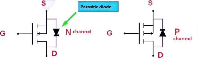
A CMOS transistor is made up of two types of devices: a P-channel MOS (PMOS) and an N-channel MOS (NMOS). Together, they form the complementary structure that gives CMOS its name. For a more detailed explanation of the CMOS transistor fabrication process, please refer to the provided link.
CMOS (Complementary Metal Oxide Semiconductor)
CMOS (Complementary Metal-Oxide-Semiconductor)
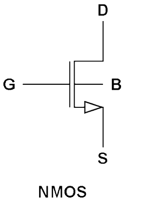
NMOS
An NMOS transistor is formed on a p-type substrate, with n-type source and drain regions diffused into it. In NMOS devices, the majority charge carriers are electrons. When a high voltage is applied to the gate, the NMOS transistor switches on and allows current to flow. Conversely, when a low voltage is applied, the device remains off and does not conduct.
NMOS technology is generally considered faster than PMOS, because electrons (the carriers in NMOS) move approximately twice as quickly as holes (the carriers in PMOS).
NMOS
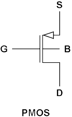
PMOS
A PMOS transistor is built with p-type source and drain regions diffused into an n-type substrate. In PMOS devices, the majority charge carriers are holes. When a high voltage is applied to the gate, the transistor remains off and does not conduct. When a low voltage is applied, the PMOS switches on and allows current to flow.
Compared with NMOS devices, PMOS transistors are generally more resistant to noise, making them advantageous in certain applications.
CMOS Working Principle
In CMOS technology, both N-type and P-type transistors work together to implement logic functions. A single input signal that switches one type of transistor on will simultaneously switch the other type off. This complementary behavior makes it possible to design logic circuits using only simple transistor switches, eliminating the need for external pull-up resistors.
In a typical CMOS logic gate, a set of n-type MOSFETs is connected in a pull-down network between the output and the low-voltage supply rail (Vss, often ground). Instead of relying on load resistors as in NMOS logic, CMOS circuits use a network of p-type MOSFETs arranged in a pull-up network between the output and the higher-voltage supply rail (commonly referred to as Vdd).
CMOS using Pull Up & Pull Down
Thus, when a p-type and n-type transistor share the same input signal at their gates, the p-type MOSFET conducts when the n-type MOSFET is off, and vice versa. The pull-up and pull-down networks are arranged so that, for any given input pattern, one network is active while the other is inactive, as illustrated in the figure below.
CMOS technology provides several key benefits: high operating speed, low power consumption, strong noise immunity in both logic states, and reliable operation across a wide range of input and supply voltages (as long as the supply voltage remains constant).
To gain a clearer understanding of how Complementary Metal-Oxide-Semiconductor circuits function, let’s take a closer look at the structure and behavior of CMOS logic gates, which are explained in the following section.
Which Devices Use CMOS?
CMOS technology is widely applied in many types of integrated circuits. It is the foundation of microcontrollers, microprocessors, SRAM (Static Random Access Memory), and various digital logic circuits. Beyond digital systems, CMOS is also used in numerous analog applications, including data converters, image sensors, and highly integrated transceivers for different communication systems.
CMOS Inverter
The CMOS inverter is one of the most fundamental circuits, shown in the figure below. It is built using both a PMOS and an NMOS transistor, with the input signal A serving as the gate voltage for both.
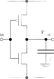
CMOS inverter
- The NMOS transistor is connected to the low-voltage rail (Vss or ground).
- The PMOS transistor is connected to the high-voltage rail (Vdd).
- The output is taken from terminal Y.
When a high voltage (~Vdd) is applied to the input terminal A, the PMOS transistor turns off (acting as an open circuit), while the NMOS transistor conducts, pulling the output down to Vss (logic 0).
When a low voltage (~0 V) is applied to the inverter input, the NMOS transistor turns off while the PMOS transistor turns on. As a result, the output is pulled up to Vdd (logic high).
| Input Voltage | Logic Input | Output Voltage | Logic Output |
|---|---|---|---|
| 0 V | 0 | Vdd | 1 |
| Vdd | 1 | 0 V | 0 |
CMOS NAND Gate
The figure below illustrates a 2-input CMOS NAND gate. It consists of:
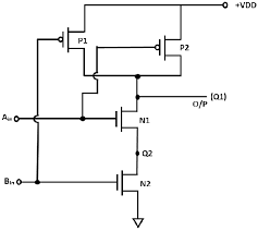
Two Input NAND Gate
- Two NMOS transistors connected in series between the output (Y) and ground.
- Two PMOS transistors connected in parallel between the output (Y) and Vdd.
Here’s how it works:
- If either input A or B is at logic 0, at least one of the NMOS transistors will be OFF, breaking the connection from Y to ground. At the same time, at least one of the PMOS transistors will be ON, establishing a path from Y to Vdd. This means the output will be pulled high (logic 1).
Hence, the output Y will be high unless both inputs are high. When A and B are both logic 1, the two NMOS transistors conduct (ON), creating a path to ground, while both PMOS transistors are OFF. As a result, the output is pulled down to logic 0.
Truth Table of CMOS NAND Gate
| A | B | Pull-Down Network | Pull-Up Network | Output Y |
|---|---|---|---|---|
| 0 | 0 | OFF | ON | 1 |
| 0 | 1 | OFF | ON | 1 |
| 1 | 0 | OFF | ON | 1 |
| 1 | 1 | ON | OFF | 0 |
CMOS NOR Gate
The figure below shows a 2-input CMOS NOR gate. Its configuration is the reverse of the NAND gate:
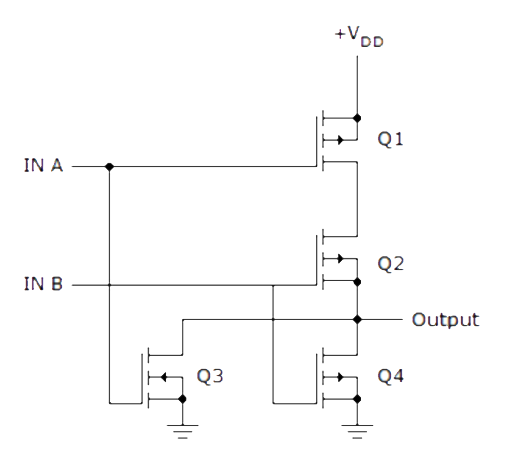
Two Input NOR Gate
- The NMOS transistors are connected in parallel, so if either input is high, the output is pulled low.
- The PMOS transistors are connected in series, so the output is pulled high only when both inputs are low.
This ensures the output is never left floating, and the operation matches the truth table shown below.
Truth Table of CMOS NOR Gate
| A | B | Y |
|---|---|---|
| 0 | 0 | 1 |
| 0 | 1 | 0 |
| 1 | 0 | 0 |
| 1 | 1 | 0 |
CMOS Fabrication
CMOS transistors are fabricated on silicon wafers, which can range in diameter from 20 mm up to 300 mm. The process is similar to lithographic printing, where in each step different materials are deposited, etched, or patterned to form circuit structures. By examining both the top view and the cross-section of the wafer, the overall process can be understood as a simplified layered assembly.
CMOS fabrication is typically carried out using one of three main technologies:
- N-well or P-well processes
- Twin-well technology
- Silicon-on-Insulator (SOI)
For a deeper explanation of the fabrication process, please refer to the provided link.
Lifetime of a CMOS Battery
The average lifespan of a CMOS battery is about 10 years, though this can vary depending on usage conditions and the environment in which the computer operates.
Failure Symptoms of a CMOS Battery
When a CMOS battery begins to fail, the computer can no longer retain its system time and date after being powered off. For example, when restarted, the machine may display a default time like 12:00 PM, January 1, 1990, which is a clear sign of battery failure.
Other common symptoms include:
- Difficulty starting up the computer or laptop
- Continuous beeping sounds from the motherboard during boot
- System time and date resetting unexpectedly
- Peripherals not functioning properly
- Missing or corrupted hardware drivers
- Inability to connect to the Internet
CMOS Characteristics
One of the most important features of CMOS technology is its very low static power consumption combined with high noise immunity. When one transistor in a CMOS pair is switched off, the overall circuit only uses significant power during the brief switching between on and off states.
Because of this, CMOS devices generate much less heat compared to other logic families like TTL or NMOS, which tend to draw a continuous current even when their outputs are stable.
These advantages allow CMOS circuits to integrate high-density logic functions on a single chip, making CMOS the preferred technology for most VLSI (Very Large Scale Integration) designs.
The term MOS refers to the physical structure of the MOSFET, where a metal gate electrode sits atop an oxide insulating layer on the semiconductor substrate.
Historically, aluminum was used as the metal gate material, but today it has largely been replaced by polysilicon. However, with the introduction of high-κ dielectric materials, the industry is revisiting the use of metal gates as part of advanced CMOS fabrication processes.
CCD vs CMOS
Charge-Coupled Devices (CCD) and Complementary Metal-Oxide-Semiconductor (CMOS) are two distinct technologies used in digital image sensors. Both convert light into electrical signals, but they differ in how they capture and process images, each with its own strengths, weaknesses, and typical applications.
The primary difference between CCD and CMOS sensors lies in their image capture method: CCDs use a global shutter, capturing the entire frame at once, while CMOS sensors typically use a rolling shutter, which captures the image line-by-line.
CCD sensors are manufactured using a specialized process that enables them to transfer charge across the chip with minimal distortion. This results in exceptionally high-quality images, with excellent light sensitivity and low noise levels.
On the other hand, CMOS sensors are made using standard manufacturing processes similar to those used for microprocessors. This makes CMOS chips generally cheaper and easier to produce. However, this also means CMOS sensors are typically more prone to noise compared to CCDs.
In terms of power consumption, CMOS sensors are much more energy-efficient—often consuming over 100 times less power than CCD sensors.
Because CMOS fabrication fits within typical silicon production lines, CMOS sensors tend to be less expensive. CCD technology, having been around longer and mass-produced for years, is more mature and established.
Both sensor types rely on the photoelectric effect to convert incoming light into electrical signals.
Due to these differences, CCDs are favored in applications requiring high-quality images, with many pixels and superior light sensitivity. CMOS sensors usually offer lower resolution, image quality, and sensitivity, although recent advances have brought CMOS technology close to matching CCD performance in some areas.
Overall, CMOS cameras are typically more affordable and offer longer battery life, making them popular for consumer electronics.
Latch-Up in CMOS
Latch-up occurs when a short circuit forms between the power supply (VDD) and ground (GND) in a CMOS circuit, causing a large current to flow that can potentially damage the IC. This happens because of unintended interaction between parasitic transistors inside the chip—specifically, parasitic PNP and NPN bipolar transistors.
Inside a CMOS device, these parasitic PNP and NPN transistors create a path connecting the two supply rails, VDD and GND. If triggered, this path acts like a low-impedance short, allowing excessive current to flow directly from power to ground.
To prevent latch-up, resistors or high-resistance elements are placed in strategic parts of the circuit to limit current flow and ensure the product of the transistor gains (β₁ × β₂) remains below 1, stopping the parasitic transistors from turning on uncontrollably.
Physically, the parasitic structure behaves like a silicon-controlled rectifier (SCR) formed around the PMOS and NMOS transistors, separated by insulating oxide layers. Modern CMOS technologies include built-in latch-up protection that detects and disables the device if latch-up is detected.
Latch-up testing is offered by many third-party vendors. The test involves attempts to deliberately trigger the parasitic SCR structure by applying power and signals to the chip’s pins, while monitoring for overcurrent conditions.
It’s recommended to send initial production samples to a certified latch-up test lab. The lab will apply maximum rated supply voltages and stimulus to input/output pins and monitor the chip’s current draw to detect any latch-up events.
Advantages of CMOS
The main advantages of CMOS over TTL (Transistor-Transistor Logic) include:
- Better noise margins and lower power consumption, since CMOS circuits avoid a direct conductive path between VDD and GND during steady states.
- Power is mainly consumed during switching, making CMOS chips energy-efficient and cost-effective.
- CMOS is commonly used to refer to the memory on a computer motherboard that stores BIOS settings such as date, time, and hardware configurations.
- CMOS outputs actively drive signals in both high and low states, improving performance.
- Operates from a single power supply (typically +VDD).
- CMOS gates are simple in design with high input impedance.
- Power dissipation is minimal when held at a constant state.
- High fan-out capability, meaning a single output can drive many inputs.
- Compatible with TTL logic levels, allowing easy interfacing.
- Good temperature stability and strong noise immunity.
- Compact, mechanically robust design.
- Large logic voltage swings (close to VDD), improving signal clarity.
Disadvantages of CMOS
Some drawbacks of CMOS technology include:
- Increased manufacturing cost if additional processing steps are required, though this can often be mitigated.
- Packing density is lower compared to NMOS technology, meaning CMOS chips may occupy more silicon area.
- CMOS devices are sensitive to static electricity; if leads are not properly shorted or protected, static discharge can damage the chip. Protective circuits are often included to prevent this.
- CMOS inverters require two transistors (both PMOS and NMOS) compared to a single transistor in NMOS inverters, leading to larger chip area usage.
However, these disadvantages have become less significant over time due to continuous advancements in CMOS technology.
CMOS Applications
Complementary MOS (CMOS) technology has become the dominant choice, effectively replacing NMOS and bipolar processes in nearly all digital logic circuits. CMOS is widely used in the design and manufacture of:
- Computer memories and CPUs
- Microprocessors
- Flash memory chips
- Application-Specific Integrated Circuits (ASICs)
CMOS transistors are popular because they are highly energy-efficient—they consume power mainly during switching and very little otherwise. The complementary action of the PMOS and NMOS transistors ensures that the output voltage is well controlled, resulting in low power consumption and minimal heat generation.
Because of these advantages, CMOS technology has replaced older designs like CCD sensors in cameras and is now used in most modern processors. Additionally, the CMOS memory in computers acts as a form of non-volatile RAM, storing BIOS settings along with the system’s date and time information.
I hope this explanation has helped you better understand CMOS technology. If you have any questions about this topic or electronics projects, feel free to share your thoughts in the comments below.
Here’s a question for you: Why is CMOS preferred over NMOS?
Frequently Ask Questions
What is the function of Complementary Metal-Oxide-Semiconductor (CMOS)?
CMOS is a technology widely used in computer processors, memory chips, and various electronic devices. Its primary role is to control and regulate electrical signals within these components, ensuring they operate correctly and efficiently.
What is CMOS and how does it work?
In computers, CMOS mainly stores essential system settings and configurations—such as the date and time, boot sequence, hardware parameters, and security passwords. This data is maintained by a small battery-powered memory chip on the motherboard, commonly known as the CMOS battery.
What are the disadvantages of CMOS?
Some drawbacks of CMOS technology include:
- Lower packing density compared to bipolar technologies, meaning fewer transistors per chip area.
- Increased manufacturing costs if the processing steps become more complex, although solutions exist to address these challenges.
Is a CMOS battery important?
Yes, the CMOS battery powers the chip that stores vital system information on your motherboard. If this battery fails or loses charge, your computer can lose important settings, which may cause startup problems and unstable operation.
Can you run a computer without a CMOS battery?
A computer can run without a CMOS battery, but it will lose all BIOS settings every time it powers down. This results in longer boot times and potential configuration errors each time the system restarts.
What is the main advantage of CMOS?
CMOS circuits offer several key benefits:
- Simple design and structure
- Low power consumption
- High noise immunity
- Strong temperature stability
- High integration capability, allowing entire circuits to be compactly integrated onto a single chip
How is CMOS used as a switch?
In CMOS logic gates, NMOS and PMOS transistors act as electronic switches. By varying the voltage applied to the transistor’s gate, the transistor switches on or off, controlling current flow and enabling logic operations. The source terminal voltage serves as the control voltage in this switching process.

Amanda Miller
Amanda Miller is a senior electronics engineer with 6 years of experience. She focuses on studying resistors, transistors, and package design in detail. Her deep knowledge helps her bring innovation and high standards to the electronics industry.
Subscribe to JMBom Electronics !


