


Guide to Nanosensors
Catalog
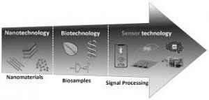
Definition of NanosensorNanosensor ComponentsNanosensor Working PrincipleNanosensor Fabrication TechniquesTypes of NanosensorsAdvantages and Disadvantages of NanosensorsApplications of NanosensorsThe first example of a nanosensor was developed in 1999 by researchers at the Georgia Institute of Technology. It was an innovative design using carbon nanotubes. A nanosensor is a specialized type of sensor, typically a tiny device built to detect and measure chemical, biological, physical, or environmental data at the nanoscale. These sensors are particularly effective for sensing applications due to their unique properties, such as an extremely high surface area to volume ratio. This article provides a quick overview of nanosensors, how they work, the different types, and their uses.
Definition of Nanosensor
A nanosensor is a type of sensor with dimensions in the nanometer range. It functions as a mechanical or chemical sensor, designed to detect nanoparticles, chemical species, or various physical parameters. Nanosensors are widely used in medical diagnostics, water quality monitoring, food testing, and chemical analysis. While they work similarly to regular sensors, they are capable of detecting very small quantities and converting these into signals that can be analyzed. Nanosensors are also applied in areas like transportation systems, pathogen detection, medicine, manufacturing, and pollution control.
Examples of nanosensors include fluorescent sensors made from DNA or peptides, carbon nanotubes, quantum dots, sensors based on plasmon coupling, magnetic resonance imaging, and photoacoustic sensors.
Nanosensor Components
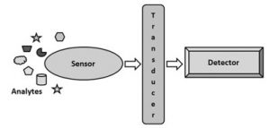
The main components of a nanosensor include the analyte, sensor, transducer, and detector. Nanosensors are capable of measuring at the single-molecule level. Typically, these sensors operate by detecting electrical changes in the sensor materials.
Nanosensor Components
In this diagram, the analyte first diffuses from the solution to the surface of the nanosensor. It then interacts specifically and efficiently, altering the physicochemical properties of the transducer's surface. This, in turn, causes a change in the transducer’s electronic or optical properties. Finally, this change is converted into an electrical signal, which is detected.
Nanosensor Working Principle
A nanosensor works by detecting electrical changes within the sensor materials. The key components of a nanosensor include the analyte, transducer, detector, and the feedback line that connects the detector to the sensor block. Nanosensors can measure at the single-molecule level, operating by detecting small electrical changes in the sensor material.
In this process, the analyte first diffuses from the solution to the surface of the sensor. It then interacts precisely and efficiently, altering the physicochemical properties of the surface. This leads to changes in the electronic or optical properties of the transducer. Ultimately, these changes are converted into an electrical signal, which is then detected.
Nanosensor History
The term "Nanosensor," originally referred to as a “Nanoprobe,” was established in 1990 based on research conducted at IBM Sindelfingen. This research focused on developing the necessary basic technologies for batch processing silicon AFM probes using bulk micromachining.
In 1993, Nanosensors commercialized AFM (Atomic Force Microscope) and SPM (Scanning Probe Microscope) probes globally. Their advancements in batch processing technology for creating AFM probes played a significant role in the introduction of Atomic Force Microscopes to the industry.
In recognition of these achievements, Nanosensors received several prestigious awards, including the Dr.-Rudolf-Eberle Innovation Award for the German State of Baden-Württemberg in 1995, the German Industry Innovation Prize, and the Förderkreis für die Mikroelektronik e.V. Innovation Award in 1999. In 2002, Nanosensors was acquired and integrated into NanoWorld, a Switzerland-based company, becoming an independent business unit.
In 2003, Nanosensors introduced an innovative new AFM-type probe, the AdvancedTEC™, which allowed precise positioning and provided Real Tip Visibility through an AFM optical system, even when the probe was slightly tilted. In the same year, NanoAndMore GmbH was appointed as Nanosensors’ official distributor for Turkey, Israel, and Europe.
In 2004, the PointProbe® Plus was launched, combining the well-established features of the PointProbe® Series, such as compatibility and high application versatility, with commercial AFMs. In 2005, the Q30K-Plus was introduced as a novel AFM probe with excellent Q-factor and enhanced S/N ratio for UHV applications.
In 2006, Nanosensors revamped its North American distribution network, and NanoAndMore USA Corp. became the official distributor for the USA, Mexico, and Canada.
In 2007, the company launched a new series of silicon MFM AFM probes, introduced the PointProbe® Plus XY-Alignment series, and unveiled the Plateau Tip AFM probes series. That year also saw the announcement of the PointProbe® Plus AFM probe Series.
In 2008, Nanosensors introduced the self-actuating and self-sensing Akiyama probe.
In 2011, the company published its first special development list and launched a new series of wear-resistant, conductive AFM probes, as well as Platinum Silicide AFM probes.
Finally, in 2013, Nanosensors introduced the uniqprobe™ AFM probe series and uploaded its first two screencasts on its YouTube channel.
Nanosensor Fabrication Techniques
Several methods are used to fabricate nanosensors, including top-down lithography, bottom-up assembly, and molecular self-assembly.
Top-Down Approaches
- Lithography: This method involves etching nanoscale patterns onto substrates using techniques such as electron beam lithography (EBL) or photolithography. EBL is particularly useful due to its high resolution, which is crucial for creating precise nanoscale features.
- Etching: Both wet and dry etching techniques are used to selectively remove material from the surface of a substrate to form nanoscale structures. Reactive ion etching (RIE) is a widely used dry etching technique known for its precision and ability to create complex patterns.
Bottom-Up Approaches
- Chemical Vapor Deposition (CVD): In this process, gaseous reactants form solid materials on substrates, creating thin films and nanostructures. Variants like plasma-enhanced CVD (PECVD) use plasma to speed up reaction rates, improving the process.
- Self-Assembly: This technique involves the spontaneous organization of molecules into structured forms. DNA nanotechnology, for example, leverages the base-pairing properties of DNA to create intricate nanostructures.
- Sol-Gel Processing: This method involves transforming a liquid 'sol' into a solid 'gel' phase, making it ideal for creating ceramic and glassy nanostructures.
Hybrid Approaches
- Nanoimprint Lithography (NIL): This combines aspects of both top-down and bottom-up techniques. It involves pressing a nanostructured mold into a polymer layer and then curing the polymer to transfer the nanoscale features.
Types of Nanosensors
Nanosensors come in various types, each designed for different applications. Below are the key types:
Physical Nanosensors
These sensors are used to measure changes in physical quantities such as velocity, temperature, pressure, electric forces, displacement, mass, and more. Physical nanosensors have a wide range of applications, both in everyday life and in various industries. For example, Nanowear Inc. uses physical nanosensors to create wearable undergarments that can detect early signs of heart failure in chronically ill patients by monitoring changes in electrical signals from the body.
Physical Type
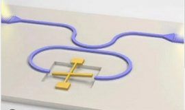
Chemical Nanosensors
Chemical nanosensors are designed to detect various chemicals or chemical properties, such as pH levels. These sensors are particularly useful in monitoring ecological pollution or conducting pharmaceutical analysis. They are typically made from nanomaterials like metal nanoparticles or graphene, which react to the presence of specific target chemicals, enabling accurate detection and measurement.
A prime example of this type of sensor is one used to detect the pH value of a liquid. A research group successfully developed such a sensor by using polymer brushes coated with gold nanoparticles, which can detect pH levels through a spectroscopic technique.
Chemical Nanosensor
Nano-Biosensors
Nano-biosensors in medicine and healthcare can precisely detect pathogens, toxins, tumors, and biomarkers. These sensors convert molecular responses into optical or electrical signals and offer the advantage of targeting exactly what needs to be measured. As the size of an object decreases and its surface-to-volume ratio increases, these sensors provide a significant advantage over larger biosensors, allowing for more frequent and accurate detection of reactions with the targeted molecules.
For example, Taiwanese start-up Instant NanoBiosensors Co., Ltd. uses optical fibers coated with gold nanoparticles and antibodies to detect various biological compounds.
Nano-biosensor
Optical Nanosensors
Optical nanosensors are made from nanoscale or nanostructured materials that react differently to electromagnetic excitation at optical frequencies. These sensors are primarily used for analytical purposes, including monitoring and identifying chemical or biological processes. They convert the observed data into signals that provide valuable information.
Optical Type
Advantages and Disadvantages of Nanosensors
Advantages:
- Nanosensors can interact at the nanoscale, allowing them to detect developments that differ from those observed at the macro level.
- They offer high sensitivity, providing greater accuracy in measurements.
- These sensors are durable, stable, portable, lightweight, and provide a robust response with real-time detection and high selectivity.
- Nanosensors consume low power, making them energy-efficient.
- They require minimal sample volumes for analysis, causing minimal disturbance to the material being observed.
- With low response times, these sensors are faster than other types, enabling real-time analysis.
- Nanosensors can detect multiple factors simultaneously, allowing for diverse applications.
- They exhibit significant ranges of detection sensitivity and resolution.
- Operating on a smaller scale, nanosensors are more sensitive and accurate.
Disadvantages:
- Nanosensors tend to be less selective for biological measurements due to the lack of high specificity for bio-receptors like DNA and antibodies.
- Top-down fabricated nanosensors have limited resolution and are typically expensive.
- Bottom-up nanosensors are often inefficient, difficult to scale, and much more expensive compared to other types.
Applications of Nanosensors
Nanosensors have a wide range of applications across various fields. Some of their key uses include:
- Plant Sciences: Nanosensors play a crucial role in plant sciences by enabling steady energy supply, detecting metabolic activities, storing and processing information, and responding to a wide range of ecological stimuli.
- Chemical, Biological, Environmental, and Physical Measurement: These sensors are designed to detect and measure chemical, biological, environmental, and physical data at the nanoscale level.
- Biomedical and Environmental Applications: Nanosensors are mechanical or chemical sensors applied in industries ranging from healthcare to environmental monitoring.
Common Applications:
- Pollution Monitoring: Nanosensors are used to detect various chemicals in gases, helping to monitor air pollution.
- Physical Parameter Monitoring: Nanosensors can measure physical parameters such as displacement, flow, and temperature.
- Plant Biology: They assist in monitoring plant signaling and metabolism to better understand plant biology.
- Neurophysiology: Nanosensors are used to study neurotransmitters in the brain, aiding in research into neurophysiology.
- MEMS Devices: These sensors are used as accelerometers in MEMS devices, such as airbag sensors.
- Agriculture: Nanosensors provide real-time measurements of soil conditions, such as pH, nutrients, moisture, and residual pesticides, benefiting agricultural practices.
- Food Safety: Nanosensors detect pesticides on fruits and vegetables, helping to identify carcinogens and ensuring food safety.
- Pathogen Detection: They are used to detect pathogens in food as part of food security and quality control.
- Metabolite Monitoring: Nanosensors detect and monitor small-molecule metabolites in various applications.
- Cancer Research: These sensors help monitor metabolic activity in cancer cells, providing real-time data on responses to therapy.
In summary, nanosensors are nanoscale devices that measure physical quantities and convert them into detectable signals for analysis. They are used in a wide range of applications in fields such as defense, healthcare, and environmental monitoring. These sensors can be fabricated using various techniques, including top-down lithography, bottom-up assembly, and molecular self-assembly.

Christopher Anderson
Christopher Anderson has a Ph.D. in electrical engineering, focusing on power electronics. He’s been a Senior member of the IEEE Power Electronics Society since 2021. Right now, he works with the KPR Institute of Engineering and Technology in the U.S. He also writes detailed, top-notch articles about power electronics for business-to-business electronics platforms.
Subscribe to JMBom Electronics !


