


ADG511/ADG512/ADG513 Precision CMOS Analog Switches
Catalog
General DescriptionProduct HighlightsFeaturesApplicationsFUNCTIONAL BLOCK DIAGRAMSElectrical CharacteristicsElectrical Characteristics (Single-Supply Operation)Ordering GuideADG511/ADG512/ADG513 PIN CONFIGURATIONTypical Performance Characteristics–ADG511/ADG512/ADG513Application: Sample-and-Hold CircuitTest CircuitsOUTLINE DIMENSIONSConclusionGeneral Description
The ADG511, ADG512, and ADG513 are monolithic CMOS ICs that incorporate four independently controlled analog switches. These switches deliver low, consistent on-resistance and support a wide analog signal range, making them well-suited for precision analog signal routing.
Manufactured with Analog Devices’ advanced LC²MOS (linear-compatible CMOS) process, they offer key advantages such as very low leakage currents, minimal power consumption, and low capacitance—enabling fast switching speeds with reduced charge injection. Thanks to these characteristics, the ADG511, ADG512, and ADG513 are excellent solutions for a broad range of precision analog signal switching applications, including signal processing and data acquisition systems.

ADG511/ADG512/ADG513
These devices can operate from a single +3 V or +5 V supply, or from ±5 V dual supplies, making them ideal for battery-powered instruments, 4–20 mA loop systems, and use with the latest generation of DACs and ADCs from Analog Devices. Running on 5 V supplies with lower operating currents, they achieve much lower power dissipation compared to traditional ±15 V devices.
The ADG511, ADG512, and ADG513 each contain four independent SPST (single-pole, single-throw) switches. The ADG511 and ADG512 differ only in their digital control logic: the ADG511 turns on with a logic low at the control input, whereas the ADG512 requires a logic high. The ADG513 combines both types of logic, with two switches operating like the ADG511 and the other two switches using inverted logic.
Product Highlights
- 5 V Single-Supply Operation The ADG511/ADG512/ADG513 deliver excellent performance with low on-resistance and a wide signal range. They are fully specified and guaranteed for operation with +3 V, +5 V, or ±5 V supply rails.
- Ultralow Power Consumption CMOS design ensures extremely low power dissipation.
- Low On-Resistance (RON) Provides precise and efficient signal switching.
- Break-Before-Make Switching Guaranteed break-before-make performance prevents channel overlap, allowing multiple outputs to be tied together safely for multiplexer applications.
Features
- Operates from +3 V, +5 V, or ±5 V power supplies
- Extremely low power dissipation (<0.5 mW)
- Very low leakage current (<100 pA)
- Low on-resistance (<50 Ω)
- Fast switching performance
- Minimal charge injection
- TTL/CMOS logic compatible
- Available in 16-lead DIP or SOIC packages
Applications
- Battery-powered instruments
- Single-supply systems
- Remotely powered equipment
- 5 V supply-based systems
- Computer peripherals, including disk drives
- High-precision instrumentation
- Audio and video switching
- Automatic test equipment
- Precision data acquisition systems
- Sample-and-hold circuits
- Communication systems
- Compatible with ±5 V supply DACs and ADCs such as AD7840/AD7848, AD7870/AD7871/AD7872/AD7874/AD7875/AD7876/AD7878
FUNCTIONAL BLOCK DIAGRAMS
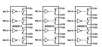
SWITCHES SHOWN FOR A LOGIC "1" INPUT
Electrical Characteristics
(typical at 25°C, unless otherwise noted)
Analog Switch
- Analog Signal Range: VDD to VSS
- On Resistance (RON): Typ: 30 Ω at VD = ±3.5 V, IS = –10 mA Max: 50 Ω at VDD = +4.5 V, VSS = –4.5 V
- Leakage Currents (VDD = +5.5 V, VSS = –5.5 V) Source Off Leakage (IS(OFF)): Typ: ±0.025 nA (VD = ±4.5 V, VS = ±4.5 V) Max: ±0.1 nA (25°C), ±2.5 nA (up to +125°C) Drain Off Leakage (ID(OFF)): Typ: ±0.025 nA Max: ±0.1 nA (25°C), ±2.5 nA (up to +125°C) Channel On Leakage (ID, IS(ON)): Typ: ±0.05 nA (VD = VS = ±4.5 V) Max: ±0.2 nA (25°C), ±5 nA (up to +125°C)
Digital Inputs
- Input High Voltage (VINH): Min 2.4 V
- Input Low Voltage (VINL): Max 0.8 V
- Input Current (IINL/IINH): Typ: 0.005 µA at VIN = VINL or VINH Max: ±0.1 µA
Dynamic Characteristics
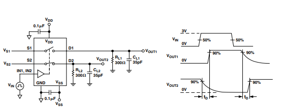
- Turn-On Time (tON): Typ 200 ns, Max 375 ns (RL = 300 Ω, CL = 35 pF, VS = ±3 V)
- Turn-Off Time (tOFF): Typ 120 ns, Max 150 ns (same test conditions)
- Break-Before-Make Time: Typ 100 ns (RL = 300 Ω, CL = 35 pF, ADG513 only)
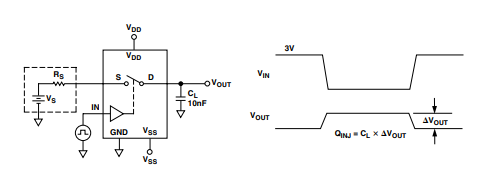
- Charge Injection: Typ 11 pC (VS = 0 V, RS = 0 Ω, CL = 10 nF)
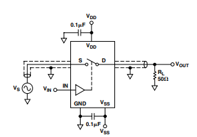
- Off Isolation: Typ 68 dB (RL = 50 Ω, CL = 5 pF, f = 1 MHz)
- Channel-to-Channel Crosstalk: Typ 85 dB (same test conditions)
- Capacitance (f = 1 MHz): CS(OFF): Typ 9 pF CD(OFF): Typ 9 pF CD, CS(ON): Typ 35 pF
Power Requirements
- VDD: +4.5 V (min) to +5.5 V (max)
- VSS: –4.5 V (min) to –5.5 V (max)
- IDD: Typ: 0.0001 µA (VDD = +5.5 V, VSS = –5.5 V) Max: 1 µA (Digital inputs = 0 V or 5 V)
- ISS: Typ: 0.0001 µA Max: 1 µA
Notes
- Temperature ranges: B Versions: –40°C to +85°C T Version: –55°C to +125°C
- Some parameters guaranteed by design, not production-tested.
- Specifications may change without notice.
Electrical Characteristics (Single-Supply Operation)
(typical at 25°C unless otherwise specified)
Analog Switch
- Analog Signal Range: 0 V to VDD
- On Resistance (RON): Typ: 45 Ω at VD = 3.5 V, IS = –10 mA Max: 75 Ω at VDD = 4.5 V
- Leakage Currents (VDD = 5.5 V) Source Off Leakage (IS(OFF)): Typ: ±0.025 nA (VD = 4.5/1 V, VS = 14.5 V) Max: ±0.1 nA (25°C), ±2.5 nA (up to +125°C) Drain Off Leakage (ID(OFF)): Typ: ±0.025 nA Max: ±0.1 nA (25°C), ±2.5 nA (up to +125°C) Channel On Leakage (ID, IS(ON)): Typ: ±0.05 nA (VD = VS = 4.5 V/1 V) Max: ±0.2 nA (25°C), ±5 nA (up to +125°C)
Digital Inputs
- Input High Voltage (VINH): Min 2.4 V
- Input Low Voltage (VINL): Max 0.8 V
- Input Current (IINL/IINH): Typ: 0.005 µA at VIN = VINL or VINH Max: ±0.1 µA
Dynamic Characteristics²
- Turn-On Time (tON): Typ 250 ns, Max 500 ns (RL = 300 Ω, CL = 35 pF, VS = 2 V)
- Turn-Off Time (tOFF): Typ 50 ns, Max 100 ns (same test conditions)
- Break-Before-Make Time: Typ 200 ns (RL = 300 Ω, CL = 35 pF, ADG513 only)
- Charge Injection: Typ 16 pC (VS = 0 V, RS = 0 Ω, CL = 10 nF)
- Off Isolation: Typ 68 dB (RL = 50 Ω, CL = 5 pF, f = 1 MHz)
- Channel-to-Channel Crosstalk: Typ 85 dB (same test conditions)
- Capacitance (f = 1 MHz): CS(OFF): Typ 9 pF CD(OFF): Typ 9 pF CD, CS(ON): Typ 35 pF
Power Requirements
- VDD: Min 4.5 V, Max 5.5 V
- IDD: Typ: 0.0001 µA (VDD = 5.5 V) Max: 1 µA (digital inputs = 0 V or 5 V)
Notes
- Temperature ranges: B Versions: –40°C to +85°C T Version: –55°C to +125°C
- Parameters guaranteed by design, not tested in production.
- Specifications may be updated without prior notice.
Ordering Guide
| Model | Temperature Range² | Package Option³ |
|---|---|---|
| ADG511BN | –40°C to +85°C | N-16 |
| ADG511BR | –40°C to +85°C | R-16A |
| ADG511ABR⁴ | –40°C to +85°C | R-16A |
| ADG511TQ⁴ | –55°C to +125°C | Q-16 |
| ADG512BN | –40°C to +85°C | N-16 |
| ADG512BR | –40°C to +85°C | R-16A |
| ADG512ABR⁴ | –40°C to +85°C | R-16A |
| ADG513BN | –40°C to +85°C | N-16 |
| ADG513BR | –40°C to +85°C | R-16A |
| ADG513ABR⁴ | –40°C to +85°C | R-16A |
Notes
- For MIL-STD-883, Class B processed parts, please contact the factory.
- Specifications for 3.3 V operation apply over the 0°C to +70°C temperature range.
- Package codes: N = Plastic DIP; R = 0.15" Small Outline IC (SOIC); Q = Cerdip.
- Trench-isolated, latch-up proof devices. See Trench Isolation section for details.
ADG511/ADG512/ADG513 PIN CONFIGURATION
(DIP/SOIC)
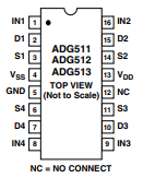
ADG511/ADG512/ADG513
Truth Table (ADG511 / ADG512)
| Control Input (ADG511) | Control Input (ADG512) | Switch Condition |
|---|---|---|
| 0 | 1 | ON |
| 1 | 0 | OFF |
Truth Table (ADG513)
| Logic Level | Switches 1 & 4 | Switches 2 & 3 |
|---|---|---|
| 0 | OFF | ON |
| 1 | ON | OFF |
Terminology
- VDD – Most positive power supply voltage.
- VSS – Most negative power supply voltage in dual-supply operation. In single-supply applications, this may be tied to ground (GND).
- GND – Ground reference (0 V).
- S (Source) – Source terminal of the switch; can serve as either input or output.
- D (Drain) – Drain terminal of the switch; can serve as either input or output.
- IN – Digital logic control input.
- RON – On resistance; resistance between D and S when the switch is conducting.
- IS(OFF) – Source leakage current when the switch is “OFF.”
- ID(OFF) – Drain leakage current when the switch is “OFF.”
- ID, IS(ON) – Channel leakage current when the switch is “ON.”
- VD (VS) – Analog voltage present at terminals D or S.
- CS(OFF) – Source capacitance of the switch when “OFF.”
- CD(OFF) – Drain capacitance of the switch when “OFF.”
- CD, CS(ON) – Switch capacitance when “ON.”
- tON – Turn-on delay; time from applying a digital control signal to the switch conducting.
- tOFF – Turn-off delay; time from applying a digital control signal to the switch turning off.
- tD – Switching delay; measured between the 90% transition points of both switches when toggling between address states (ADG513 only).
- Crosstalk – Undesired signal coupling from one channel to another due to parasitic capacitance.
- Off Isolation – A measure of signal attenuation through a switch in the “OFF” state.
- Charge Injection – Transient charge transferred from the digital control input to the analog output during switching.
Typical Performance Characteristics–ADG511/ADG512/ADG513
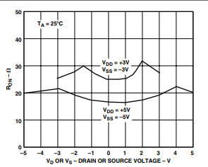
TPC 1. On Resistance as a Function of VD (VS) Dual
Supplies
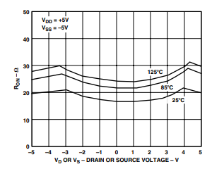
TPC 2. On Resistance as a Function of VD (VS) for
Different Temperatures
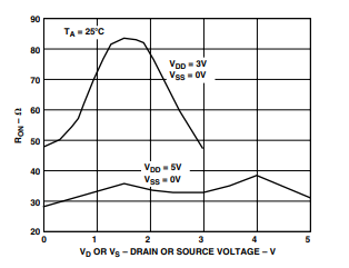
TPC 3. On Resistance as a Function of VD (VS)
Single Supply
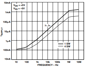
TPC 4. Supply Current vs. Input Switching Frequency
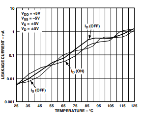
TPC 5. Leakage Currents as a Function of Temperature
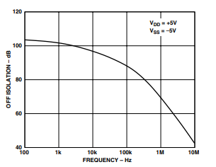
TPC 6. Off Isolation vs. Frequency
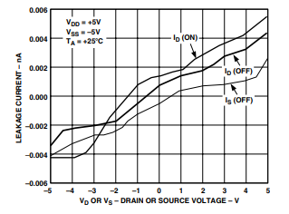
TPC 7. Leakage Currents as a Function of VD (VS)
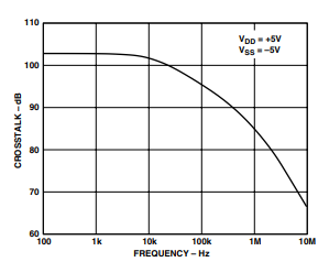
TPC 8. Crosstalk vs. Frequency
Application: Sample-and-Hold Circuit
- The setup uses an AD845 as the input buffer and an OP07 as the output amplifier.
- Track mode (SW1 closed): Output VOUTV_{OUT}VOUT directly follows the input signal VINV_{IN}VIN.
- Hold mode (SW1 open): The capacitor CHC_HCH stores the voltage. Some leakage occurs, but the ADG511/512/513’s low leakage minimizes voltage droop. Using a polystyrene capacitor further reduces the droop (around 15 µV/µs typical).
Extra Design Tricks
- SW2 in parallel with SW1: Helps cancel out pedestal error by balancing potentials → reduces charge injection.
- RC + CC compensation network: Cuts pedestal error further. Reduces hold-time glitches. Optimizes acquisition time.
Performance
- Pedestal error: max 5 mV (for ±3 V input range).
- Acquisition time: ~2.5 µs.
- Settling time: ~1.85 µs.
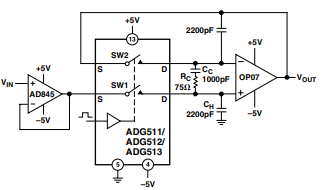
Figure 1. Accurate Sample-and-Hold
Trench Isolation
- The MOSFETs inside the ADG511A/512A/513A are separated by an oxide trench layer. This physical barrier keeps devices electrically isolated from each other.
Why this matters:
- Without proper isolation, latch-up can occur.
- Latch-up happens when parasitic P-N junctions between CMOS transistors turn forward-biased, allowing large, uncontrolled currents to flow → which can damage or destroy the device.
Junction Isolation vs. Trench Isolation
- Junction Isolation (older method): Uses N-well and P-well diodes to keep devices apart. Works under normal conditions since the diode is reverse biased. But during overvoltage, that diode goes forward biased → triggers a parasitic SCR (Silicon-Controlled Rectifier) structure. Result: current amplification → latch-up.
- Trench Isolation (modern method): Removes that parasitic diode by using an oxide trench instead. Prevents SCR formation. End result: Latch-up proof circuit.
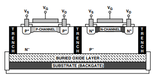
Figure 2. Trench Isolation
Test Circuits
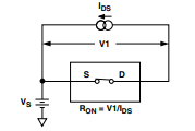
Test Circuit 1. On Resistance
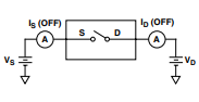
Test Circuit 2. Off Leakage
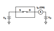
Test Circuit 3. On Leakage
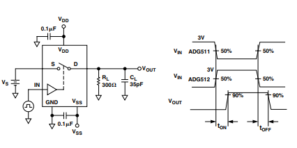
Test Circuit 4. Switching Times
Test Circuit 5. Break-Before-Make Time Delay
Test Circuit 6. Charge Injection
Test Circuit 7. Off Isolation
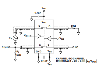
Test Circuit 8. Channel-to-Channel Crosstalk
OUTLINE DIMENSIONS
Dimensions shown in inches and (mm).
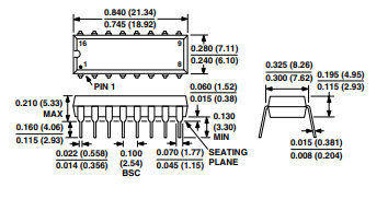
16-Lead Plastic DIP
(N-16)
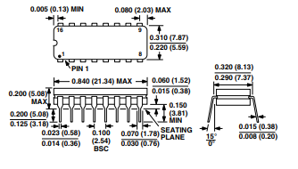
16-Lead Cerdip
(Q-16)
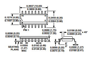
16-Lead SOIC
(R-16A)
Conclusion
The ADG511, ADG512, and ADG513 are precision, low-leakage CMOS analog switches with fast switching, low on-resistance, and excellent off-isolation. Trench isolation makes them latch-up proof, and their flexible supply options and low power consumption make them ideal for high-accuracy signal switching in data acquisition, sample-and-hold, and precision instrumentation applications.

Christopher Anderson
Christopher Anderson has a Ph.D. in electrical engineering, focusing on power electronics. He’s been a Senior member of the IEEE Power Electronics Society since 2021. Right now, he works with the KPR Institute of Engineering and Technology in the U.S. He also writes detailed, top-notch articles about power electronics for business-to-business electronics platforms.
Subscribe to JMBom Electronics !


