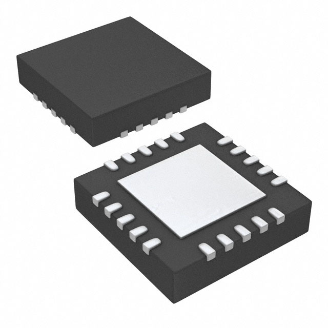
NXP ADC0808S250HW/C1,1


- Part Number:
ADC0808S250HW/C1,1
- Manufacturer:
- Category:
- RoHs:
 RoHS Compliant
 - Datasheet:
 ADC0808S250HW/C1,1_Datesheet
 - Description:
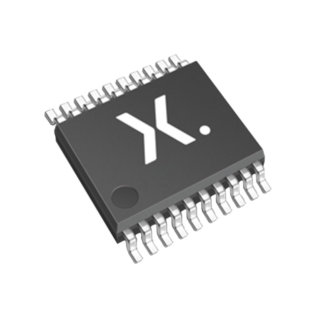
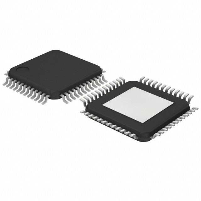
IC ADC 8BIT 48HTQFP
- In stock 0

ADC0808S250HW/C1 Product Information
Overview
The ADC0808S250HW/C1 is a high-speed, 8-bit Analog-to-Digital Converter (ADC) optimized for telecommunication transmission control systems and tape drive applications. It supports a sampling frequency of up to 250 MHz, making it suitable for demanding applications requiring high-speed data acquisition.
Key Features
- 8-bit Resolution: Provides precise digital representation of analog signals.
- High-Speed Sampling: Supports sampling rates up to 250 MHz.
- Maximum Analog Input Frequency: Up to 560 MHz.
- Programmable Acquisition Output Clock: Allows adjustment of acquisition clock delay and frequency.
- Differential Analog Input: Enhances signal integrity and noise rejection.
- Integrated Voltage Regulator: For analog input full-scale control or external reference.
- Selectable Clock Input: Supports 1.8 V CMOS or LVDS clock inputs.
- 1.8 V CMOS Digital Outputs: Compatible with modern digital systems.
- Binary or 2’s Complement Outputs: Offers flexibility in data representation.
- Low Latency: Only 2 clock cycles.
- Industrial Temperature Range: -40 °C to +85 °C.
- HTQFP48 Package: Suitable for high-density PCB layouts.
Applications
- 2.5G and 3G Cellular Base Infrastructure Radio Transceivers: Ideal for high-speed data conversion in communication systems.
- Wireless Access Systems: Enhances performance in wireless networking applications.
- Fixed Telecommunications: Provides reliable data conversion for fixed-line systems.
- Optical Networking: Supports high-speed data transmission in optical networks.
- Wireless Local Area Network (WLAN) Infrastructure: Enhances data acquisition in WLAN systems.
- Tape Drive Applications: Ensures accurate data conversion for tape storage systems.
Ordering Information
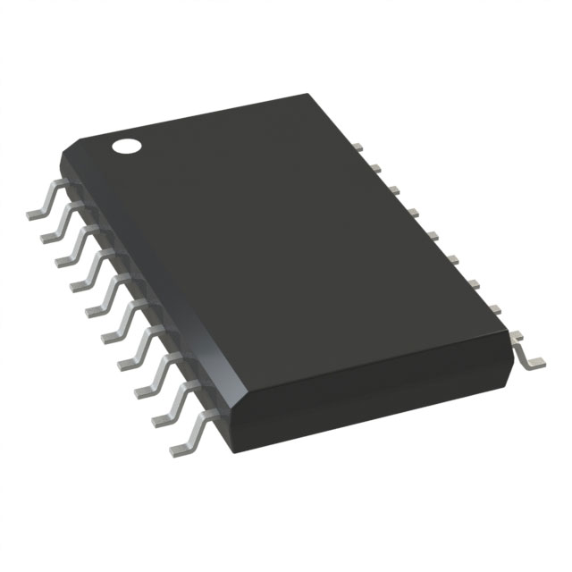
- Type Number: ADC0808S250HW/C1
- Sampling Frequency: 250 MHz
- Package: HTQFP48
- Description: Plastic thermally enhanced thin quad flat package with 48 leads
Pinning Information
Pin Configuration
- OGND1: Data output ground 1
- D3: Data output bit 3
- VCCO1(1V8): Data output supply voltage 1 (1.8 V)
- D4: Data output bit 4
- OGND2: Data output ground 2
- D5: Data output bit 5
- VCCO2(1V8): Data output supply voltage 2 (1.8 V)
- D6: Data output bit 6
- VCCO3(1V8): Data output supply voltage 3 (1.8 V)
- D7: Data output bit 7
- CCS: Complete conversion signal output
- CE_N: Chip enable input (active LOW)
- IR: In-range output
- OTC: Control input for 2’s complement output
- DGND1: Digital ground 1
- VCCD1(1V8): Digital supply voltage 1 (1.8 V)
- CCSSEL: Control input for CCS frequency selection
- NC1V8: Not connected or connected to VCCD1(1V8)
- AGND1: Analog ground 1
- CMADC: Regulator common-mode ADC output
- FSIN/REFSEL: Full-scale reference voltage input/internal reference selection
- AGND2: Analog ground 2
- INN: Complementary analog input
- IN: Analog input
- VCCA1(3V3): Analog supply voltage 1 (3.3 V)
- CLKSEL: Control input for clock input selection
- CLK+: Clock input
- CLK−: Complementary clock input
- DEL0: Complete conversion signal delay input 0
- DEL1: Complete conversion signal delay input 1
- D0: Data output bit 0
- VCCO4(1V8): Data output supply voltage 4 (1.8 V)
- D1: Data output bit 1
- D2: Data output bit 2
- DGND: Digital ground; exposed die pad
Functional Description
CMOS/LVDS Clock Input
- LVDS Mode: Differential LVDS levels with an external resistor of 80 Ω to 120 Ω.
- 1.8 V CMOS Mode: Sampling on the rising edge of the clock input signal with CLK− grounded.
Digital Output Coding
- Output Formats: Binary or 2’s complement.
- Output Levels: 1.8 V CMOS compatible.
Timing Output
- Output Delay: Up to 6.9 ns for LVDS clock input.
- Output Hold Time: 3.3 ns to 4.8 ns for LVDS clock input.
Complete Conversion Signal
- Adjustable CCS Signal: Controlled by DEL0 and DEL1 for optimal data acquisition timing.
Full-Scale Input Selection
- Internal Reference: Enabled by connecting FSIN to ground, providing a common-mode output voltage of 0.95 V.
- External Reference: Allows adjustment of the ADC input range with an external reference voltage applied to FSIN.
Limiting Values
- Analog Supply Voltage (VCCA): -0.5 V to +4.6 V
- Digital Supply Voltage (VCCD): -0.5 V to +2.5 V
- Output Supply Voltage (VCCO): -0.5 V to +2.5 V
- Input Voltage (Vi(IN), Vi(INN)): -0.5 V to VCCA + 1 V
- Clock Input Voltage (Vi(CLK)): -0.5 V to VCCD + 0.55 V
- Storage Temperature (Tstg): -55 °C to +150 °C
- Ambient Temperature (Tamb): -40 °C to +85 °C
- Junction Temperature (Tj): - to 150 °C
Thermal Characteristics
- Thermal Resistance (Rth(j-a)): 36.2 K/W
- Thermal Resistance (Rth(j-c)): 14.3 K/W
Static Characteristics
- Analog Supply Current (ICCA): Up to 60 mA at 125 MHz
- Digital Supply Current (ICCD): Up to 12 mA at 125 MHz
- Output Supply Current (ICCO): Up to 11 mA at 125 MHz
- Total Power Dissipation (Ptot): Up to 240 mW at 125 MHz
Dynamic Characteristics
- Clock Frequency (fclk): 1 MHz to 250 MHz
- Output Delay Time (td(o)): 5.4 ns to 7.3 ns for 1.8 V CMOS clock input
- Output Hold Time (th(o)): 3.3 ns to 4.8 ns for 1.8 V CMOS clock input
- Integral Non-Linearity (INL): ±0.82 LSB at 20 MHz clock frequency
- Differential Non-Linearity (DNL): ±0.4 LSB at 20 MHz clock frequency
- Offset Error (EO): ±2.5 mV at 25 °C ambient temperature
- Gain Error (EG): ±1.85% at 25 °C ambient temperature
- Bandwidth (B): Up to 560 MHz at -3 dB
- Total Harmonic Distortion (THD): -53 dB at 125 MHz clock frequency
- Signal-to-Noise Ratio (S/N): 47 dBc to 48 dBc at 125 MHz clock frequency
- Spurious Free Dynamic Range (SFDR): 55 dBc at 125 MHz clock frequency
- Intermodulation Distortion (IMD): -55 dB for second-order and -60 dB for third-order
Package Outline
- Package Type: HTQFP48
- Dimensions: Refer to the detailed package outline in the datasheet for exact dimensions.
Purchase
No need to register to order from JMBom Electronics, but signing in lets you track your order like a pro. Give it a try for a smoother shopping ride.
Means
Easy peasy! Pay your way with PayPal, Credit Card, or wire transfer in USD. We've got you covered.
RFQ(Request for Quotations)
Get the freshest prices and stock updates by asking for a quote! Our sales team will shoot you an email within a day. It's that simple.
IMPORTANT NOTICE
1. Look out for your order details in your inbox! (If it's missing, check the spam folder just in case.)
2. Our sales manager will double-check the order and keep you posted on any price or stock changes. No worries, we've got you covered.

Shipping Rate
We ship orders once a day around 5 p.m., except Sunday. Once shipped, the estimated delivery time depends on the courier company you choose, usually 5-7 working days.

Shipping Methods
We provide DHL, FedEx, UPS, EMS, SF Express, and Registered Air Mail international shipping.


Payment
You can pay the orders on the website directly or pay by wire transfer offline. We support: Paypal、VISA、Credit Card.