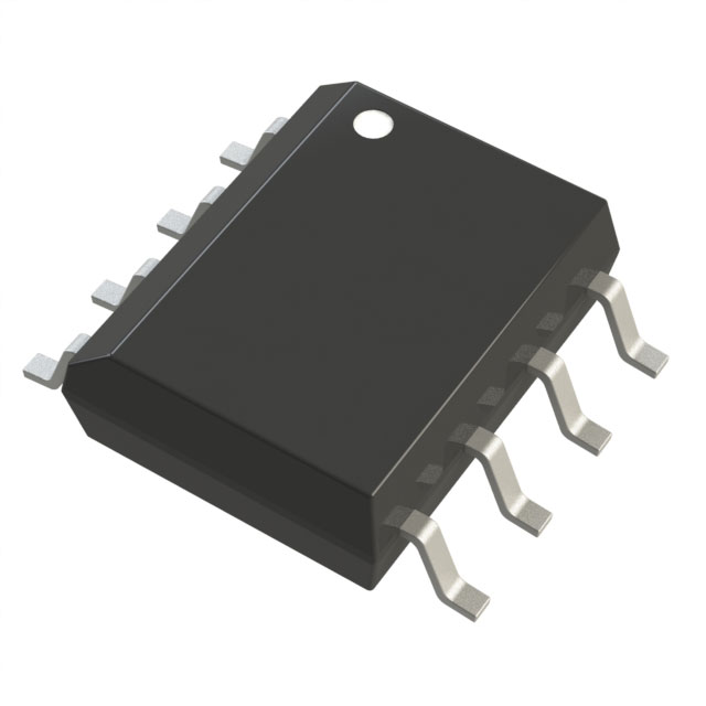
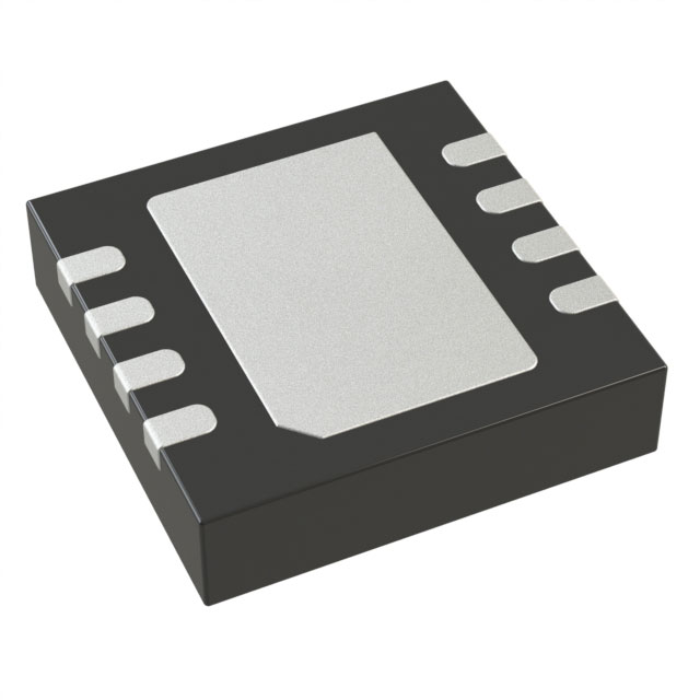
Infineon Technologies CY27410LTXI-016T


- Part Number:
CY27410LTXI-016T
- Manufacturer:
- Category:
- RoHs:
 Non-RoHS Compliant
 - Datasheet:
- Description:
INFINEON
- In stock 0
CY27410LTXI-016T – 4-PLL Spread-Spectrum Clock Generator
Infineon (formerly Cypress) – Complete Technical & Ordering Summary
1. Device Identity
| Attribute | Detail |
|---|---|
| Orderable Part Number | CY27410LTXI-016T |
| Base Type Number | CY27410 |
| Description | 4-PLL programmable clock generator, 12 outputs, industrial temperature, factory pre-configured |
| Configuration Code | -016 (customer-specific frequency set, contact factory) |
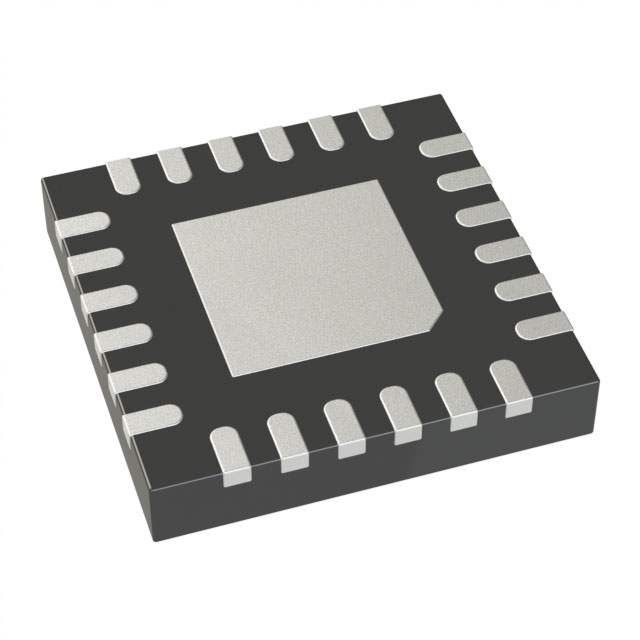
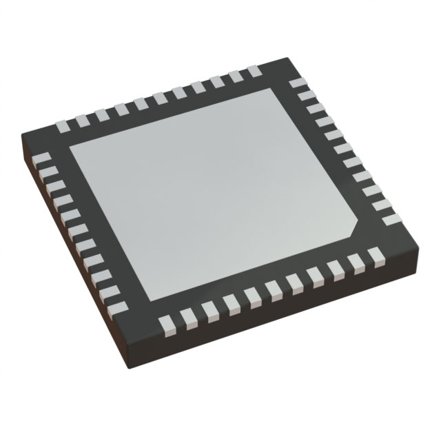
| Package | 48-pin QFN (7 × 7 × 1.0 mm) |
| Shipping Method | 13-inch tape-and-reel (T suffix) |
| RoHS Status | Lead-free / RoHS-compliant (X = Pb-free) |
| Temperature Grade | Industrial (−40 °C to +85 °C) |
2. Package & Mechanical Data
- Package Name: QFN-48 “LT” (Cypress designation)
- JEDEC Code: MO-220 variation
- Body Size: 7.0 mm × 7.0 mm × 1.0 mm max.
- Lead Pitch: 0.5 mm
- Exposed Pad (E-PAD): 5.6 × 5.6 mm – must be soldered to ground for electrical & thermal performance
- MSL Rating: MSL-3, 260 °C peak-reflow compatible
- PCB Footprint: Available in Altium, Cadence, Mentor libraries (Infineon AN72845)
3. Electrical Highlights
- Core Supply (VDD): 1.71 V – 1.89 V (1.8 V ±5 %), 2.25 V – 2.75 V (2.5 V ±10 %), 3.13 V – 3.46 V (3.3 V ±5 %)
- I/O Supply (VDDIO_x): Independent 1.8 / 2.5 / 3.3 V domains for each output bank
- PLL Count: 4 independent fractional-N PLLs (Frac-N)
- RMS Phase Jitter: 1 ps max (12 kHz – 20 MHz offset, 156.25 MHz LVDS)
- Output Frequency Ranges:LVDS / LVPECL / CML / HCSL: 25 MHz – 700 MHzLVCMOS: 3 MHz – 250 MHzLow-frequency counter: 1 kHz – 8 MHz (one pin)
- Input References:Crystal: 8 – 48 MHz (8 pF – 12 pF load)LVCMOS: 8 – 250 MHzDifferential: 8 – 700 MHz (AC-coupled)
- Spread Spectrum: 0.1 % – 5 % down/center, 0.1 % steps, 30 – 60 kHz modulation
- VCXO Mode: ±120 ppm pull-range on PLL1 (0.23 ppm/step) via VIN pin (0 – VDD)
- Output Skew: ≤100 ps (differential pairs within same bank, same PLL)
- Power Consumption:26.5 mA typ per PLL (includes dividers)13.25 mA typ per LVDS pair (100 Ω load)38 mA max core current (all PLLs active)
4. Functional Features
- Zero-Delay Buffer (ZDB): Feedback on IN2 for <±250 ps propagation delay
- Non-Zero Delay Buffer (NZDB): PLL-bypass mode for level-translation only
- Frequency-Select (FS0-FS2): 3-pin hardware frequency switching among 8 pre-loaded configurations
- I²C Interface: 400 kHz Fast-mode, 7-bit address (default 0x69), supports on-board reprogramming
- Output Enable (OE): Individual pin control or I²C register for power-down / standby
- Phase Adjustment: 0 – 4 VCO-cycle programmable delay per output
- Crystal Oscillator: Integrated load caps & feedback resistor, supports 8 – 48 MHz crystals (Table 2 specs)
5. Compliance & Standards
| Protocol | Specification Met |
|---|---|
| PCIe | Gen 1/2/3 (HCSL 100 MHz, <1 ps RMS jitter) |
| USB | 2.0 / 3.0 (24 MHz, 48 MHz, 60 MHz) |
| SATA | 1.0 / 2.0 (75 MHz, 150 MHz) |
| 10-GbE | 156.25 MHz (LVPECL / LVDS) |
| Spread-Spectrum | Lexmark & logic profiles, EMI reduction |
6. Absolute Maximum Ratings
- VDD / VDDIOx: −0.5 V to +4.6 V
- VI (any pin): −0.5 V to VDD+0.4 V
- I²C pins: −0.5 V to +6 V
- Storage Temp: −55 °C to +150 °C
- TJ max: +100 °C
- ESD HBM: 2 kV
- Latch-up: 140 mA (JESD78)
7. Thermal & Reliability
| Parameter | Value | Unit | Condition |
|---|---|---|---|
| θJA | 15.64 | °C/W | Still air, JEDEC 51 |
| θJC | 2.21 | °C/W | Junction-to-case |
| Data Retention | 10 | Years | NV memory @ 55 °C |
| Programming Cycles | 100 k | Cycles | NV memory |
8. Ordering Information
| Part Number | Description | Package | Temp. | Flow |
|---|---|---|---|---|
| CY27410LTXI-016T | Factory-configured, -016 profile | 48-QFN | −40 to +85 °C | Tape & Reel |
| CY27410FLTXI | Field-programmable (blank) | 48-QFN | −40 to +85 °C | Tray |
| CY27410FLTXIT | Field-programmable (blank) | 48-QFN | −40 to +85 °C | Tape & Reel |
Note: “-016” is a customer-specific frequency plan; contact Infineon for exact output frequencies, or use ClockWizard 2.1 to generate the configuration file.
9. Design Resources
- Datasheet: 001-89074 Rev. *M (Feb-2019)
- ClockWizard 2.1: Free GUI for config & OTP programming
- AN72845: QFN layout & thermal guidelines
- IBIS Model: Available on Infineon website
- Evaluation Kit: CY27410EVAL (socketed QFN + USB-I²C bridge)
Purchase
No need to register to order from JMBom Electronics, but signing in lets you track your order like a pro. Give it a try for a smoother shopping ride.
Means
Easy peasy! Pay your way with PayPal, Credit Card, or wire transfer in USD. We've got you covered.
RFQ(Request for Quotations)
Get the freshest prices and stock updates by asking for a quote! Our sales team will shoot you an email within a day. It's that simple.
IMPORTANT NOTICE
1. Look out for your order details in your inbox! (If it's missing, check the spam folder just in case.)
2. Our sales manager will double-check the order and keep you posted on any price or stock changes. No worries, we've got you covered.

Shipping Rate
We ship orders once a day around 5 p.m., except Sunday. Once shipped, the estimated delivery time depends on the courier company you choose, usually 5-7 working days.

Shipping Methods
We provide DHL, FedEx, UPS, EMS, SF Express, and Registered Air Mail international shipping.


Payment
You can pay the orders on the website directly or pay by wire transfer offline. We support: Paypal、VISA、Credit Card.


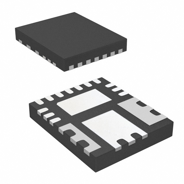
Infineon Technologies
Infineon Technologies
Infineon Technologies
Infineon Technologies

Infineon Technologies
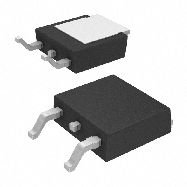
Infineon Technologies

Infineon Technologies

Infineon Technologies

Infineon Technologies
Infineon Technologies
Infineon Technologies
Infineon Technologies

