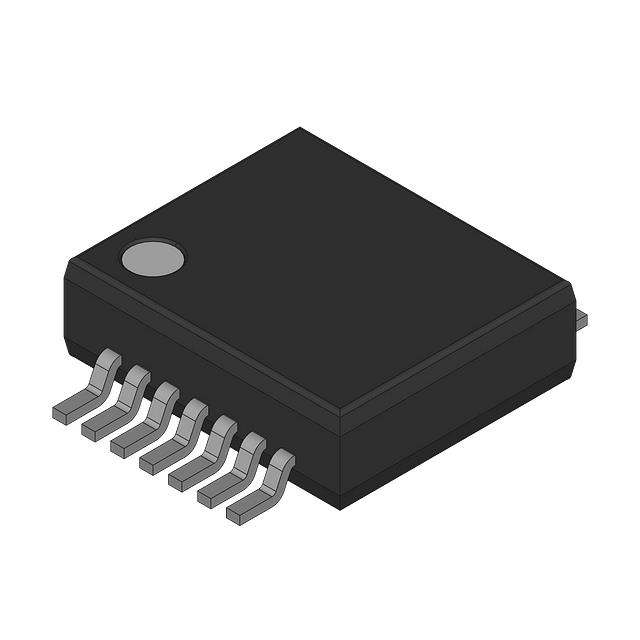
NXP SAF7751EL/N207ZK


- Part Number:
SAF7751EL/N207ZK
- Manufacturer:
- Category:
- RoHs:
 Non-RoHS Compliant
 - Datasheet:
- Description:
CAR DSP
- In stock 0

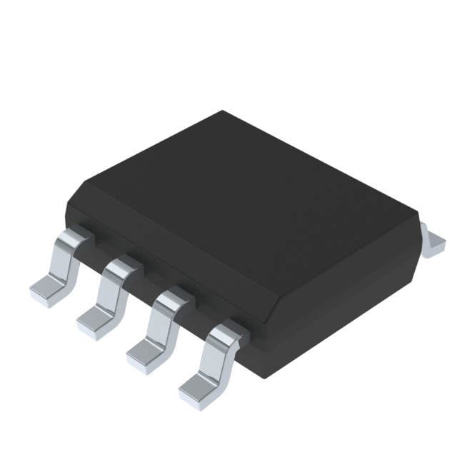
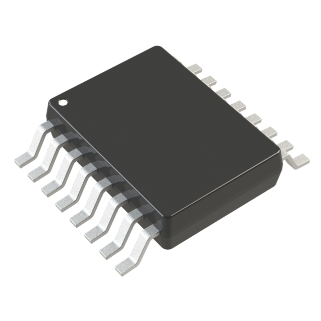
NX5DV330PW Model Information
General Description
The NX5DV330PW is a quad 1-of-2 high-speed TTL-compatible video multiplexer/demultiplexer. It features low ON resistance, allowing inputs to be connected to outputs without adding propagation delay or generating additional ground bounce noise. The device includes a digital select input (S), four independent inputs/outputs (nY0, nY1), a common input/output (nZ), and an active LOW enable input (E). Schmitt-trigger action at the enable input (E) and select input (S) ensures tolerance to slower input rise and fall times across the entire VCC range from 4.0 V to 5.5 V.
Features
- 5 Ω switch connection between two ports
- TTL-compatible input levels
- Minimal propagation delay through the switch
- ESD protection:HBM JESD22-A114E Class 2A exceeds 2000 VMM JESD22-A115-A exceeds 200 VCDM JESD22-C101C exceeds 1000 V
- Latch-up testing exceeds 100 mA (JEDEC standard JESD78)
- Operating temperature range: -40 °C to +85 °C
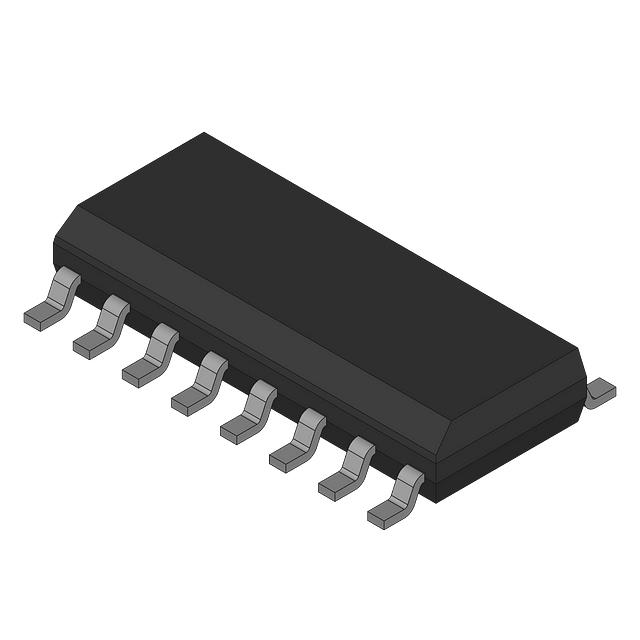
Ordering Information
- Type number: NX5DV330PW
- Package: TSSOP16 (plastic thin shrink small outline package; 16 leads; body width 4.4 mm)
- Temperature range: -40 °C to +85 °C
Pinning Information
Pin Configuration
- S: Select control input
- 1Y0, 1Y1, 2Y0, 2Y1, 3Y0, 3Y1, 4Y0, 4Y1: Independent input or output
- 1Z, 2Z, 3Z, 4Z: Independent input or output
- GND: Ground (0 V)
- E: Enable input (active LOW)
- VCC: Positive supply voltage
Pin Description
TableCopy
| Symbol | Pin | Description |
|---|---|---|
| S | 1 | Select control input |
| 1Y0 | 2 | Independent input or output |
| 1Y1 | 3 | Independent input or output |
| 1Z | 4 | Independent input or output |
| 2Y0 | 5 | Independent input or output |
| 2Y1 | 6 | Independent input or output |
| 2Z | 7 | Independent input or output |
| GND | 8 | Ground (0 V) |
| E | 15 | Enable input (active LOW) |
| VCC | 16 | Positive supply voltage |
| 4Y0 | 14 | Independent input or output |
| 4Y1 | 13 | Independent input or output |
| 4Z | 12 | Independent input or output |
| 3Y0 | 11 | Independent input or output |
| 3Y1 | 10 | Independent input or output |
| 3Z | 9 | Independent input or output |
Functional Description
The NX5DV330PW operates based on the control inputs E and S. The switch can be turned off when pin E is HIGH. The select input S determines the connection between the inputs/outputs and the common input/output.
Function Selection Table
TableCopy
| Input | Switch | |
|---|---|---|
| E | S | |
| L | L | Y0 to Z or Z to Y0 |
| L | H | Y1 to Z or Z to Y1 |
| H | X | Switch off |
Limiting Values
- Supply voltage (VCC): -0.5 V to +7.0 V
- Input voltage (VI): -0.5 V to +7.0 V
- Continuous switch current (ISW): 128 mA
- Input clamping current (IIK): -50 mA (for VI < 0 V)
- Storage temperature (Tstg): -65 °C to +150 °C
- Total power dissipation (Ptot): 500 mW (derates linearly with temperature for different packages)
Recommended Operating Conditions
- Supply voltage (VCC): 4.0 V to 5.5 V
- HIGH-level input voltage (VIH): 2.0 V
- LOW-level input voltage (VIL): 0.8 V
- Hysteresis voltage (VH): 45 mV
- Ambient temperature (Tamb): -40 °C to +85 °C
Static Characteristics
- Input clamping voltage (VIK): -1.2 V (for VCC = 4.5 V, II = -18 mA)
- Input leakage current (II): ±1 µA (for VCC = 5.5 V, VI = GND or 5.5 V)
- OFF-state leakage current (IS(OFF)): ±1 µA
- Power-off leakage current (IOFF): ±1 µA
- Supply current (ICC): 3 µA (typical)
- Additional supply current (∆ICC): 2.5 mA (typical)
- Input capacitance (CI): 3.5 pF
- OFF-state input/output capacitance (Cio(off)): 6.0 pF (Z port), 4.0 pF (Y port)
- ON-state input/output capacitance (Cio(on)): 14 pF
- ON resistance (RON): 3 Ω to 10 Ω (depending on voltage and current conditions)
Dynamic Characteristics
- Turn-on time (ton): 4.0 ns to 6.0 ns
- Turn-off time (toff): 2.3 ns to 6.0 ns
Additional Dynamic Characteristics
- Differential gain (Gdif): 0.64% (typical)
- Differential phase (ϕdif): 0.1° (typical)
- -3 dB frequency response (f(-3dB)): 300 MHz
- Isolation (OFF-state) (αiso): -60 dB to -63 dB
- Crosstalk (Xtalk): between switches
Package Outline
- TSSOP16: plastic thin shrink small outline package; 16 leads; body width 4.4 mm
Abbreviations
- CDM: Charged Device Model
- ESD: ElectroStatic Discharge
- HBM: Human Body Model
- MM: Machine Model
- TTL: Transistor-Transistor Logic
Purchase
No need to register to order from JMBom Electronics, but signing in lets you track your order like a pro. Give it a try for a smoother shopping ride.
Means
Easy peasy! Pay your way with PayPal, Credit Card, or wire transfer in USD. We've got you covered.
RFQ(Request for Quotations)
Get the freshest prices and stock updates by asking for a quote! Our sales team will shoot you an email within a day. It's that simple.
IMPORTANT NOTICE
1. Look out for your order details in your inbox! (If it's missing, check the spam folder just in case.)
2. Our sales manager will double-check the order and keep you posted on any price or stock changes. No worries, we've got you covered.

Shipping Rate
We ship orders once a day around 5 p.m., except Sunday. Once shipped, the estimated delivery time depends on the courier company you choose, usually 5-7 working days.

Shipping Methods
We provide DHL, FedEx, UPS, EMS, SF Express, and Registered Air Mail international shipping.


Payment
You can pay the orders on the website directly or pay by wire transfer offline. We support: Paypal、VISA、Credit Card.