Qorvo SPF5043Z


- Part Number:
SPF5043Z
- Manufacturer:
- Category:
- RoHs:
 Non-RoHS Compliant
 - Datasheet:
 SPF5043Z_Datesheet
 - Description:
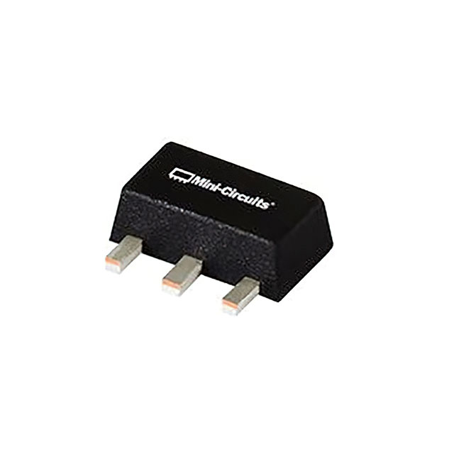
RF Amplifier IC Cellular, ISM, PCS 50MHz ~ 4GHz SOT-343
- In stock 25

SPF5043Z – Complete Datasheet Summary
1. Basic Device Information
- Part Number: SPF5043Z
- Manufacturer: Qorvo
- Device Type: GaAs pHEMT MMIC Low-Noise Amplifier (LNA)
- Frequency Range: 50 MHz to 4000 MHz
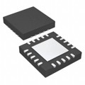
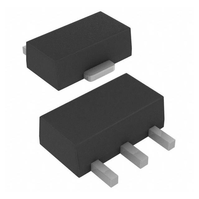
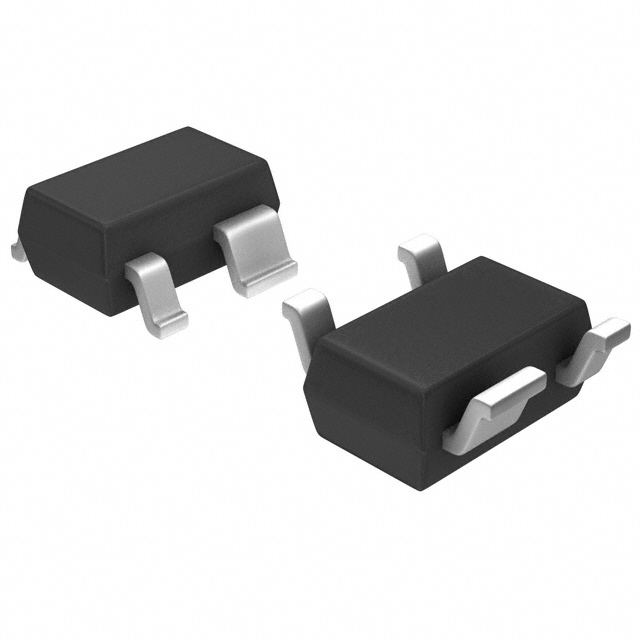
- Package: SOT‑343 (4‑pin, miniature SOT‑343 surface‑mount)
- Supply Voltage: 3 V to 5 V single supply
- Quiescent Current: 46 mA (typ at 5 V); 25 mA (typ at 3 V)
- Internal Matching: 50 Ω input/output matched
- ESD Rating: HBM Class 1A
- Moisture Sensitivity: MSL 1 (unlimited floor life)
- RoHS: Compliant (lead‑free, halogen‑free, antimony‑free)
- Datasheet Revision: June 12, 2018
2. Key Features
- Ultra‑low noise figure: 0.8 dB typ @ 900 MHz
- High gain: 18.2 dB @ 900 MHz; 12.9 dB @ 1960 MHz
- High linearity: OIP3 up to 38.5 dBm
- High output P1dB: 22.7 dBm @ 1900 MHz
- Integrated active bias for stable current over temperature
- Broadband 50 Ω internal matching
- Single‑supply operation (3–5 V)
- Compact SOT‑343 package
- Excellent reverse isolation
- ESD and robust handling
3. Electrical Specifications (TA = 25°C, VD = 5 V, IDQ = 46 mA, 50 Ω)
Key Performance
| Parameter | Condition | Min | Typ | Max | Unit |
|---|---|---|---|---|---|
| Frequency Range | — | 50 | — | 4000 | MHz |
| Small‑Signal Gain | @ 900 MHz | 16.7 | 18.2 | 19.7 | dB |
| @ 1960 MHz | 11.4 | 12.9 | 14.4 | dB | |
| Noise Figure | @ 900 MHz | — | 0.8 | 1.0 | dB |
| @ 1900 MHz | — | 0.8 | — | dB | |
| Output P1dB | @ 900 MHz | 17.4 | 22.6 | — | dBm |
| @ 1900 MHz | — | 22.7 | — | dBm | |
| OIP3 | @ 900 MHz | 30.0 | 33.0 | — | dBm |
| @ 1900 MHz | — | 35.0 | — | dBm | |
| Reverse Isolation | @ 900 MHz | — | 23.5 | — | dB |
| Input Return Loss | @ 900 MHz | 13.0 | 16.0 | — | dB |
| Output Return Loss | @ 900 MHz | 13.0 | 17.5 | — | dB |
| Drain Current | — | — | 46 | 54 | mA |
Absolute Maximum Ratings
| Parameter | Rating | Unit |
|---|---|---|
| Drain Voltage (VD) | +5.5 | V |
| Drain Current (ID) | 100 | mA |
| CW Input Power | +25 | dBm |
| Power Dissipation | 330 | mW |
| Storage Temperature | −65 to +150 | °C |
| Operating Temperature | −40 to +85 | °C |
| Junction Temperature | 150 | °C |
4. Pin Configuration (SOT‑343, Top View)
| Pin No. | Name | Function |
|---|---|---|
| 1 | RF Out | RF output; drain bias input |
| 2 | GND | DC/RF ground |
| 3 | RF In | RF input (internally DC‑coupled) |
| 4 | GND | DC/RF ground |
5. Typical Performance Summary
At VD = 5 V, ID = 46 mA
- Gain: 23.5 dB @ 100 MHz → 7.0 dB @ 3.8 GHz
- NF: 0.61 dB @ 400 MHz → 1.49 dB @ 3.8 GHz
- OIP3: 30.5 dBm @ 100 MHz → 38.5 dBm @ 3.5 GHz
- Output P1dB: ~22.5–23.1 dBm across band
At VD = 3 V, ID = 25 mA
- Gain: 22.6 dB @ 100 MHz → 6.7 dB @ 3.8 GHz
- NF: 0.60 dB @ 100 MHz → 1.48 dB @ 3.8 GHz
- OIP3: 26.5 dBm @ 100 MHz → 33.5 dBm @ 3.5 GHz
- Output P1dB: ~19.3–20.3 dBm across band
6. Functional Description
- GaAs pHEMT high‑gain, low‑noise device
- Active bias stabilizes quiescent current vs. voltage and temperature
- Internal matching eliminates external matching components
- Single supply simplifies biasing (VD applied at pin 1 RF Out)
- DC‑coupled input requires external DC blocking capacitor
- Output requires DC blocking cap
7. Application Circuit Requirements
- Input DC blocking capacitor: 100 pF (C3)
- Output DC blocking capacitor: 100 pF (C1, C4)
- Drain supply decoupling: 0.1 μF (C2)
- RF choke: 100 nH (L1) for bias feeding
- Evaluation board: SPF5043ZPCK1 (50 MHz–4000 MHz)
8. Applications
- Cellular, PCS, W‑CDMA, LTE, ISM
- High‑dynamic‑range receivers
- Wideband LNA and gain blocks
- Portable and battery‑powered radios
- Test equipment frontends
9. Packaging & Ordering
- SPF5043Z: 3000 units on 7‑inch reel
- SPF5043ZSR: 100 units on 7‑inch reel
- SPF5043ZPCK1: Evaluation board + 5‑pc sample bag
10. Layout & Reliability
- SOT‑343 land pattern with solid ground plane
- Short, direct RF traces; minimize parasitics
- Backside paddle soldered to ground for thermal/electrical performance
- Lead‑free reflow compatible (max 260°C)
- ESD sensitivity: Class 1A; proper handling required
Purchase
No need to register to order from JMBom Electronics, but signing in lets you track your order like a pro. Give it a try for a smoother shopping ride.
Means
Easy peasy! Pay your way with PayPal, Credit Card, or wire transfer in USD. We've got you covered.
RFQ(Request for Quotations)
Get the freshest prices and stock updates by asking for a quote! Our sales team will shoot you an email within a day. It's that simple.
IMPORTANT NOTICE
1. Look out for your order details in your inbox! (If it's missing, check the spam folder just in case.)
2. Our sales manager will double-check the order and keep you posted on any price or stock changes. No worries, we've got you covered.

Shipping Rate
We ship orders once a day around 5 p.m., except Sunday. Once shipped, the estimated delivery time depends on the courier company you choose, usually 5-7 working days.

Shipping Methods
We provide DHL, FedEx, UPS, EMS, SF Express, and Registered Air Mail international shipping.


Payment
You can pay the orders on the website directly or pay by wire transfer offline. We support: Paypal、VISA、Credit Card.