
Microchip Technology SY604JZ


- Part Number:
SY604JZ
- Manufacturer:
- Category:
- RoHs:
 RoHS Compliant
 - Datasheet:
 SY604JZ_Datesheet
 - Description:
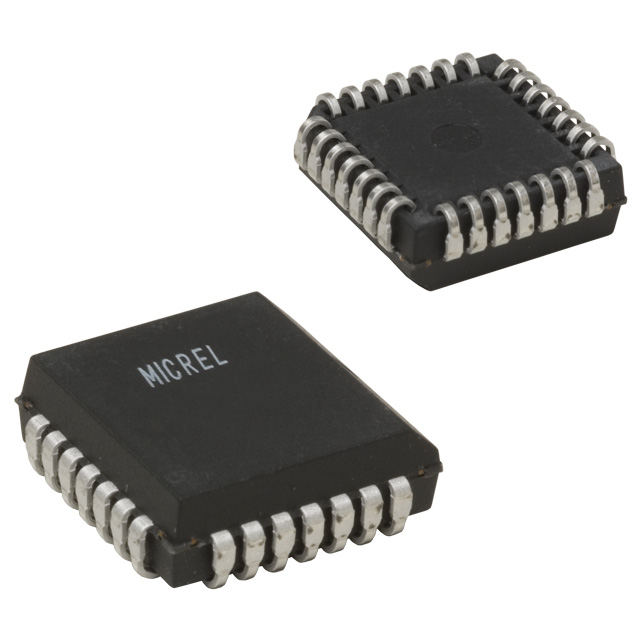
IC DELAY LINE 255TAP PROG 28PLCC
- In stock 0

Technical Specifications for SY604JZ
General Information
- Part Number: SY604JZ
- Description: 125MHz Trigger Programmable Timing Edge Vernier
- Package Type: J28-1 (28-pin Plastic Leaded Chip Carrier)
- Operating Range: Commercial
- Revision: E
- Issue Date: May 1998
Features
- True 125MHz retrigger rate
- Pin-compatible with BT604
- 15ps delay resolution
- Less than ±1LSB timing accuracy
- Differential TRIGGER inputs
- Delay spans from 4 to 40ns
- Compatible with 10K ECL logic
- Lower power dissipation: 350mW typical
- Available in 28-pin plastic (PLCC) or metal (MLCC) J-lead package
Block Diagram
- D0 - D7: 8-bit Latch DAC PULSE GEN OUT VBB4 CE LINEAR D RAMP GENERATOR FF (0 = STOP, 1 = RUN) TRIG R IEXT
Description
Micrel-Synergy's SY604 is an ECL-compatible timing vernier (delay generator) whose time delay is programmed via an 8-bit code which is loaded concurrently with the circuit trigger. The SY604 is fabricated in Micrel-Synergy's proprietary ASSET™ bipolar process.
The device can be retriggered at speeds up to 125MHz, with a delay span as short as 4ns. At minimum span, the resolution is 4ns/255 = 15.7ps per step. The delay span is externally adjustable up to 40ns. The SY604 employs differential TRIGGER inputs and produces a differential OUTPUT pulse; all other control signals are single-ended ECL. Edge delay is specified by an 8-bit input which is loaded into the device with the TRIGGER. The output pulse width will typically be 3.5ns.
The SY604 is commonly used in Automatic Test Equipment to provide precise timing edge placement; it is also found in many instrumentation and communications applications.
Pin Configuration
- D0-D7: Data input pins (ECL compatible). On the rising edge of TRIG, a ramp is initiated whereupon D0-D7 are latched into the device. D0 is the LSB. These inputs specify the amount of delay from the rising edge of TRIG to the output.
- CE: Chip enable input (ECL compatible). CE must be a logical zero on the rising edge of TRIG to enable the device to respond to the trigger. If CE is floating, the trigger will always be enabled.
- TRIG, TRIG: Differential trigger inputs (ECL compatible). The rising edge of TRIG is used to trigger the delay cycle if CE is a logical zero. If CE is a logical one, no operation occurs. It is recommended that triggering be performed with differential inputs.
- OUT, OUT: Differential outputs (ECL compatible).
- IEXT: Current reference pin. The amount of current sourced into this pin determines the span of output delay.
- COMP1, COMP2: Compensation pins. A 0.1μF ceramic capacitor must be connected between COMP1 and VEE0, and COMP2 and VEE0.
- VEE: Device power. All VEE pins must be connected.
- VCC: Device ground. All VCC pins must be connected.
- VBB: -1.36V (typical)
Functional Description
The output pulse generation cycle begins with the arrival of TRIG. When TRIG transitions to a high and CE is low, the values on D0-D7 are latched, thereby setting the DAC values. Simultaneously with the latching of D0-D7, the linear ramp generator is initiated. When the ramp level reaches that of the DAC, the comparator initiates the pulse generator to produce an output pulse of fixed width. The generation of an output pulse resets the ramp and the cycle is ready to begin again.
Absolute Maximum Ratings
- VEE: Power Supply (VCC = 0V): -8 to 0V
- VI: Input Voltage (VCC = 0V): 0 to VEE
- IOUT: Output Current: 50mA (continuous), 100mA (surge)
- TA: Operating Temperature Range: 0 to +85°C
- VEE: Operating Range: -5.7 to -4.2V
DC Characteristics
- VIH: Input HIGH Voltage (10K): -1.170V to -0.840V (typical)
- VIL: Input LOW Voltage (10K): -1.950V to -1.480V (typical)
- VOH: Output HIGH Voltage (10K): -1.020V to -0.840V (typical)
- VOL: Output LOW Voltage (10K): -1.950V to -1.630V (typical)
- IIH: Input High Current (Vin = VIH max): 100µA to 150µA
- IIL: Input Low Current (Vin = VIL min): 100µA to 150µA
- Differential Linearity Error: ±0.84LSB to ±0.9LSB
- Integral Linearity Error: ±0.89LSB to ±1.25LSB
- VBB Output Voltage: -1.44V to -1.25V
- IEXT for Tspans: See table for specific values based on Tspan
- VEE Supply Current: Up to 100mA
AC Characteristics
- fMAX: Trigger Rate: Up to 125MHz
- tWI: Trigger Width High: 2.0ns to 1.0ns
- tWO: Output Pulse Width High Time: 2.5ns to 4.5ns
- Output Pulse Rise/Fall Time: 550ps to 750ps
- tS: Output Pulse Spacing: 8.0ns (for 4ns span)
- Minimum Delay Time vs. Tspan: See table for specific values
- Output Delay: 4.0ns to 40ns
- 1 LSB Resolution: 15.7ps to 157ps
- Temperature Coefficient: ±2ps/°C
- Power Supply Rejection: 60ps/V
Application Diagram
- REXT Calculation: REXT = (VEXT + 1.25V) / IEXT
- Example: For Tspan around 15ns, IEXT is around 0.6mA. REXT = 2.08K ohms
Ordering Information
- Ordering Code: SY604JC (J28-1 package, Commercial range)
- Package Type: J28-1 (28-pin Plastic Leaded Chip Carrier)
- Operating Range: Commercial
Package Dimensions
- 28-lead PLCC (J28-1): Detailed dimensions provided in the datasheet
Purchase
No need to register to order from JMBom Electronics, but signing in lets you track your order like a pro. Give it a try for a smoother shopping ride.
Means
Easy peasy! Pay your way with PayPal, Credit Card, or wire transfer in USD. We've got you covered.
RFQ(Request for Quotations)
Get the freshest prices and stock updates by asking for a quote! Our sales team will shoot you an email within a day. It's that simple.
IMPORTANT NOTICE
1. Look out for your order details in your inbox! (If it's missing, check the spam folder just in case.)
2. Our sales manager will double-check the order and keep you posted on any price or stock changes. No worries, we've got you covered.

Shipping Rate
We ship orders once a day around 5 p.m., except Sunday. Once shipped, the estimated delivery time depends on the courier company you choose, usually 5-7 working days.

Shipping Methods
We provide DHL, FedEx, UPS, EMS, SF Express, and Registered Air Mail international shipping.


Payment
You can pay the orders on the website directly or pay by wire transfer offline. We support: Paypal、VISA、Credit Card.


Microchip Technology
Microchip Technology
Microchip Technology
Microchip Technology
Microchip Technology
Microchip Technology
Microchip Technology
Microchip Technology
Microchip Technology
Microchip Technology
Microchip Technology
Microchip Technology