
Texas Instruments(TI) TLV61046ADBVT


- Part Number:
TLV61046ADBVT
- Manufacturer:
- Category:
- RoHs:
 RoHS Compliant
 - Datasheet:
 TLV61046ADBVT_Datesheet
 - Description:
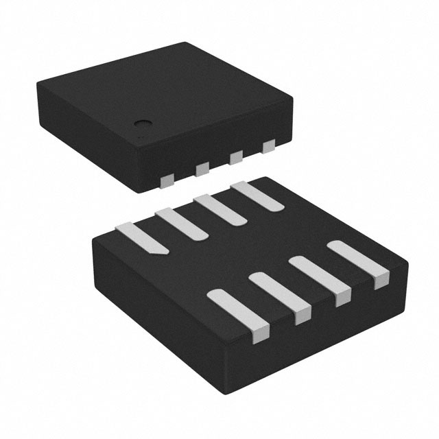
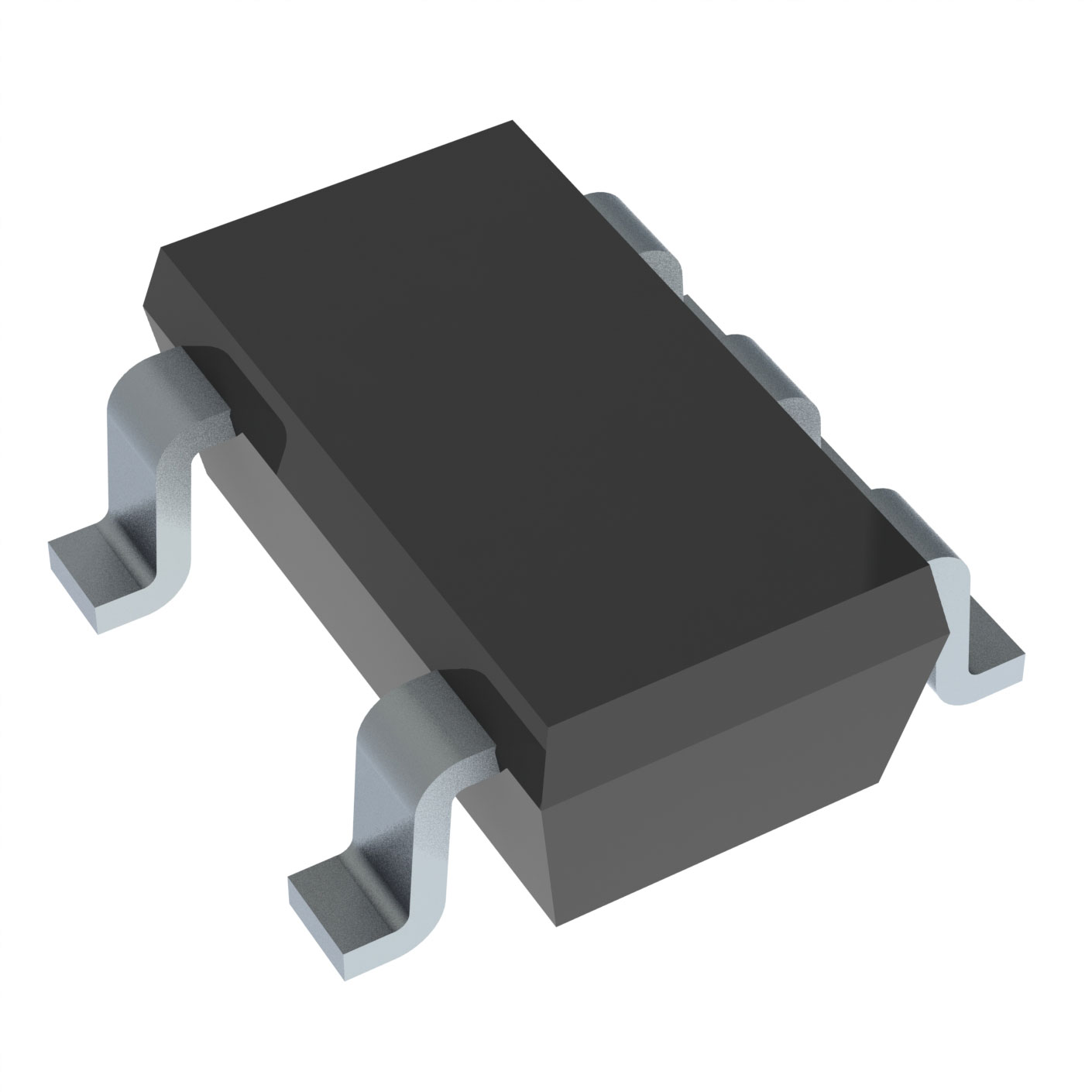
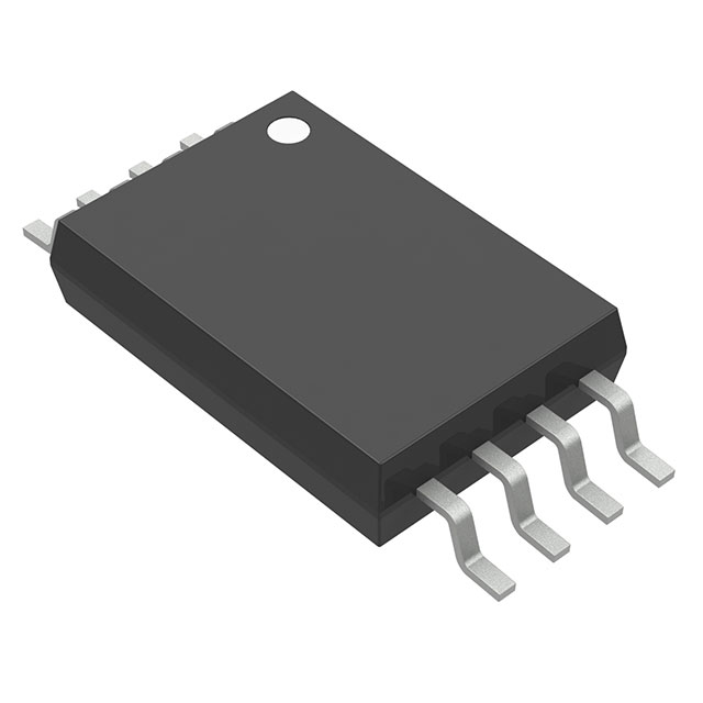
IC REG BOOST ADJ SOT23-6
- In stock 24,132

TLV61046ADBVT: Technical Specifications and Details
Overview
The TLV61046ADBVT is a highly-integrated boost converter designed for applications requiring high voltage and small solution size, such as PMOLED panel power supply and sensor modules. This product is manufactured by Texas Instruments and is RoHS compliant and Pb-Free. The data sheet was last revised in February 2021.
Features
- Input Voltage Range: 1.8 V to 5.5 V, down to 1.6 V after start-up
- Output Voltage: Up to 28 V
- Integrated Power Diode and Isolation Switch
- 980-mA (typical) Switch Current
- Up to 85% Efficiency at 3.6-V input and 12-V output
- ±2.5% Output Voltage Accuracy
- Power Save Operation Mode at Light Load
- Internal 7-ms Soft Start Time
- True Disconnection Between Input and Output During Shutdown
- Output Short Circuit Protection
- Output Overvoltage Protection
- Thermal Shutdown Protection
- 3-mm × 3-mm SOT23-6 Package
Applications
- PMOLED Power Supply
- LCD Panel
- Wearable Devices
- Portable Medical Equipment
- Sensor Power Supply
Pin Configuration and Functions
| Pin | Type | Description |
|---|---|---|
| SW | PWR | Switch pin of the converter, connected to the drain of the internal power MOSFET |
| GND | PWR | Ground |
| FB | I | Voltage feedback of adjustable output voltage, connected to the center tap of a resistor divider to program the output voltage |
| EN | I | Enable logic input, logic high voltage enables the device, logic low voltage disables the device and turns it into shutdown mode |
| VOUT | PWR | Output of the boost converter |
| VIN | I | IC power supply input |
Absolute Maximum Ratings
| Parameter | Min | Max | Unit |
|---|---|---|---|
| Voltage range at terminals (VIN, EN, FB) | -0.3 | 6 | V |
| Voltage range at terminals (SW, VOUT) | -0.3 | 32 | V |
| Operating junction temperature range (TJ) | -40 | 150 | °C |
| Storage temperature range (Tstg) | -65 | 150 | °C |
ESD Ratings
| Parameter | Value | Unit |
|---|---|---|
| Human body model (HBM) | ±2000 | V |
| Charged device model (CDM) | ±500 | V |
Recommended Operating Conditions
| Parameter | Min | Typ | Max | Unit |
|---|---|---|---|---|
| VIN Input voltage range | 1.8 | - | 5.5 | V |
| VOUT Output voltage range | 3.3 | - | 28 | V |
| L Effective inductance range | 2.2×0.7 | - | 22×1.3 | µH |
| CIN Effective input capacitance range | 0.22 | - | 1.0 | µF |
| COUT Effective output capacitance range | 0.22 | - | 10 | µF |
| TJ Operating junction temperature | -40 | - | 125 | °C |
Thermal Information
| Thermal Metric | Value | Unit |
|---|---|---|
| RθJA Junction-to-ambient thermal resistance | 177.7 | °C/W |
| RθJC(top) Junction-to-case (top) thermal resistance | 120.6 | °C/W |
| RθJB Junction-to-board thermal resistance | 33.2 | °C/W |
| ψJT Junction-to-top characterization parameter | 21.5 | °C/W |
| ψJB Junction-to-board characterization parameter | 32.6 | °C/W |
Electrical Characteristics
| Parameter | Test Conditions | Min | Typ | Max | Unit |
|---|---|---|---|---|---|
| VIN Input voltage range | - | 1.8 | - | 5.5 | V |
| VIN_UVLO Under voltage lockout threshold (VIN rising) | - | 1.75 | - | 1.8 | V |
| VIN_UVLO Under voltage lockout threshold (VIN falling) | - | 1.55 | - | 1.6 | V |
| VIN_HYS VIN UVLO hysteresis | - | - | 200 | mV | |
| IQ_VIN Quiescent current into VIN pin (IC enabled, no load, no switching) | - | 110 | 200 | µA | |
| ISD Shutdown current into VIN pin (IC disabled) | - | 0.1 | 1.0 | µA | |
| VOUT Output voltage range | - | 3.3 | - | 28 | V |
| VOUT_12V 12-V output voltage accuracy (FB pin connected to VIN pin) | 11.7 | 12.1 | 12.4 | V | |
| VREF Feedback voltage (PWM mode, TA=25°C) | 0.783 | 0.795 | 0.807 | V | |
| VOVP Output overvoltage protection threshold | 28 | 29.2 | 30.4 | V | |
| VOVP_HYS Over voltage protection hysteresis | - | - | 0.9 | V | |
| IFB_LKG Leakage current into FB pin (TA = 25°C) | - | - | 200 | nA | |
| ISW_LKG Leakage current into SW pin (IC disabled, TA = 25°C) | - | - | 500 | nA | |
| RDS(on) Isolation MOSFET on resistance (VOUT = 12 V) | - | 850 | - | mΩ | |
| Low-side MOSFET on resistance (VOUT = 12 V) | - | 450 | - | mΩ | |
| fSW Switching frequency (VIN = 3.6 V, VOUT = 12 V, PWM mode) | 850 | 1050 | 1250 | kHz | |
| tON_min Minimal switch on time | 150 | 250 | - | ns | |
| ILIM_SW Peak switch current limit (VIN = 3.6 V, VOUT = 12 V) | 680 | 980 | 1250 | mA | |
| ILIM_CHG Pre-charge current (VIN = 3.6 V, VOUT = 0 V) | 30 | 50 | - | mA | |
| tSTARTUP Startup time (VOUT from VIN to 12 V, COUT_effective = 2.2 µF, IOUT = 0 A) | 2 | 5 | - | ms | |
| VEN_H EN Logic high threshold | - | 1.2 | - | V | |
| VEN_L EN Logic Low threshold | - | 0.4 | - | V | |
| TSD Thermal shutdown threshold (TJ rising) | - | 150 | - | °C | |
| TSD_HYS Thermal shutdown hysteresis (TJ falling below TSD) | - | 20 | - | °C |
Detailed Description
The TLV61046A integrates a 30-V power switch, an input to output isolation switch, and a rectifier diode. It can output up to 28 V from an input of a Li+ battery or two alkaline batteries in series. The device operates with a switching frequency at 1.0 MHz, allowing the use of small external components. The TLV61046A has an internal default 12-V output voltage setting by connecting the FB pin to the VIN pin, requiring only three external components to achieve 12-V output voltage.
Application and Implementation
Typical Application - 12-V Output Boost Converter
- Input Voltage: 2.7 V to 4.2 V
- Output Voltage: 12 V
- Output Current: 50 mA
- Output Voltage Ripple: ±50 mV
Design Requirements
| Parameter | Value |
|---|---|
| Input Voltage | 2.7 V to 4.2 V |
| Output Voltage | 12 V |
| Output Current | 50 mA |
| Output Voltage Ripple | ±50 mV |
Custom Design with WEBENCH® Tools
- Input Voltage (VIN): 2.7 V to 4.2 V
- Output Voltage (VOUT): 12 V
- Output Current (IOUT): 50 mA
- Optimize for: Efficiency, footprint,
Purchase
No need to register to order from JMBom Electronics, but signing in lets you track your order like a pro. Give it a try for a smoother shopping ride.
Means
Easy peasy! Pay your way with PayPal, Credit Card, or wire transfer in USD. We've got you covered.
RFQ(Request for Quotations)
Get the freshest prices and stock updates by asking for a quote! Our sales team will shoot you an email within a day. It's that simple.
IMPORTANT NOTICE
1. Look out for your order details in your inbox! (If it's missing, check the spam folder just in case.)
2. Our sales manager will double-check the order and keep you posted on any price or stock changes. No worries, we've got you covered.

Shipping Rate
We ship orders once a day around 5 p.m., except Sunday. Once shipped, the estimated delivery time depends on the courier company you choose, usually 5-7 working days.

Shipping Methods
We provide DHL, FedEx, UPS, EMS, SF Express, and Registered Air Mail international shipping.


Payment
You can pay the orders on the website directly or pay by wire transfer offline. We support: Paypal、VISA、Credit Card.


Texas Instruments(TI)
Texas Instruments(TI)
Texas Instruments(TI)
Texas Instruments(TI)
Texas Instruments(TI)
Texas Instruments(TI)
Texas Instruments(TI)
Texas Instruments(TI)
Texas Instruments(TI)
Texas Instruments(TI)
Texas Instruments(TI)

Texas Instruments(TI)