


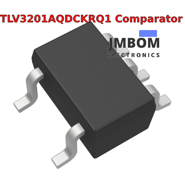
TLV3201AQDCKRQ1 Comparator: Pinout, Operation, and Typical Uses
Catalog
OverviewWhat Is the TLV3201AQDCKRQ1 Comparator?Pin Configuration of TLV3201AQDCKRQ1TLV3201AQDCKRQ1 Pin Description and Function OverviewKey Features and Technical SpecsCircuit Diagram of TLV3201AQDCKRQ1Using TLV3201 as a Comparator with HysteresisApplicationsTLV3201 Voltage Comparator: SummaryRelated ArticlesOverview
A voltage comparator is an electronic component designed to compare an input voltage against a fixed reference voltage. It switches its output depending on whether the input is higher or lower than the reference. This function is critical in detecting zero crossings, signal thresholds, and whether a voltage lies inside or outside a specific range. Comparators generally fall into two types: inverting and non-inverting. Variants include single-threshold, window, hysteresis, and three-state comparators.This article introduces the TLV3201AQDCKRQ1 voltage comparator, explaining its operation, specifications, pin configuration, and practical applications.
What Is the TLV3201AQDCKRQ1 Comparator?

TLV3201AQDCKRQ1 Voltage Comparator
The TLV3201AQDCKRQ1 is a single-channel, automotive-grade comparator that delivers both ultra-low power consumption (40 µA) and fast switching speed (40 ns) in a compact package. It offers key features such as:
- Low input offset voltage (1 mV)
- Rail-to-rail input range
- High output drive capability
The TLV320x-Q1 family includes:
- TLV3201-Q1: Single-channel version (5-pin SC70 package)
- TLV3202-Q1: Dual-channel version (8-pin VSSOP package), both with push-pull outputs for efficient switching.
Pin Configuration of TLV3201AQDCKRQ1
This comparator includes five pins, each serving a specific function:

| Pin | Name | Description |
|---|---|---|
| 1 | OUT | Comparator output |
| 2 | GND | Ground |
| 3 | IN+ | Non-inverting input |
| 4 | IN− | Inverting input |
| 5 | VCC | Positive supply voltage |
TLV3201AQDCKRQ1 Pin Description and Function Overview
Pin 1 (OUT) – Output
This pin delivers the comparator’s output signal. For accurate logic level communication with other circuit elements, proper signal routing is essential. Minimizing noise on this pin is crucial to maintain overall system reliability, a detail often underestimated but vital for stable performance.
Pin 2 (GND) – Ground
As the electrical reference for the entire circuit, the ground pin plays a foundational role. Using solid grounding techniques—such as low-impedance paths and avoiding ground loops—helps improve signal accuracy and reduce electrical interference, contributing to the precision of sensitive applications.
Pin 3 (IN+) – Non-Inverting Input
This pin receives the positive (non-inverting) input signal. Signal clarity here is key to achieving accurate voltage comparisons, particularly in environments prone to electromagnetic interference. Shielding techniques and differential routing can help preserve signal quality.
Pin 4 (IN–) – Inverting Input
The inverting input requires careful biasing to avoid offset-related errors. Reliable performance at voltage threshold crossings depends on proper component selection and board layout, making this pin’s design a critical factor in achieving high comparator accuracy.
Pin 5 (VCC) – Supply Voltage
This pin provides the device with operating power. Placing decoupling capacitors close to the VCC pin helps suppress power fluctuations, improving the comparator’s response time and stability—especially under noisy or rapidly switching conditions.
Key Features and Technical Specs
- Manufacturer: Texas Instruments
- Output Type: Push-pull
- Supply Voltage Range: 2.7V – 5.5V
- Typical Propagation Delay: 40 ns
- Low Quiescent Current: 40 µA per channel
- Rail-to-Rail Input Range: Extends 200 mV beyond either supply rail
- Input Offset Voltage: ~1 mV
- Package Type: 5-pin SC70
- Input Bias Current: Max 0.005 µA
- CMRR (Common-Mode Rejection Ratio): 70 dB
- PSRR (Power Supply Rejection Ratio): 85 dB
- Built-in Hysteresis: 1.2 mV
- Operating Temperature: –40°C to 125°C
- Mounting Style: Surface mount
Circuit Diagram of TLV3201AQDCKRQ1
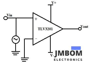
Circuit Diagram of TLV3201AQDCKRQ1
The TLV3201AQDCKRQ1 is configured like a standard comparator with push-pull output and two inputs: inverting (–) and non-inverting (+).
In the example shown, the input signal is a 1 MHz sine wave with a 200 mV peak amplitude.
- When the non-inverting input is greater than the inverting input, the output is high (e.g., 2.5V).
- When the non-inverting input is lower than the inverting input, the output goes low (e.g., –2.5V).
This comparator features a 40 ns response time, which is the delay between an input threshold crossing and output change. This fast switching speed enables high-frequency signal detection and processing. A 1.2 mV internal hysteresis improves noise immunity, avoiding false triggering due to small signal fluctuations.
Using TLV3201 as a Comparator with Hysteresis
Hysteresis helps prevent unwanted rapid switching near the threshold by requiring different input levels to turn the output on and off. It's especially useful in noisy environments.
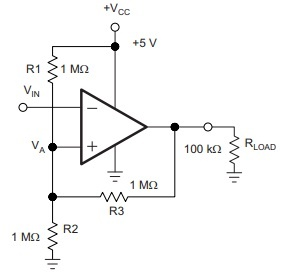
Inverting Comparator with Hysteresis
This configuration uses a three-resistor network (R1, R2, R3) to create upper and lower threshold voltages:
- When Vin < VA1, output goes high.
- When Vin > VA2, output goes low.
The resistor values determine the switching points based on feedback from the output to the input.
Non-Inverting Comparator with Hysteresis
This version uses two resistors and a fixed reference voltage applied to the inverting input. The output switches based on whether the non-inverting input is above or below the calculated threshold levels. The hysteresis in this setup prevents oscillation near the switching point.
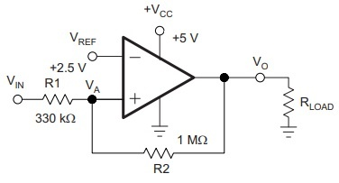
Non-inverting Comparator with Hysteresis
Understanding VIN Thresholds and Hysteresis in a Comparator Circuit
When the input voltage (VIN) drops below a certain level, the comparator’s output also goes low. To change the output state from low to high, VIN must increase to a specific threshold, referred to as VIN1. This threshold can be calculated using the following formula:
VIN1 = R1 × (VREF / R2) × VREF
Once VIN exceeds this threshold, the comparator’s output will switch to high. To return the output to a low state, VIN must fall to a second threshold — essentially the point where node 'VA' again equals VREF. This lower threshold, VIN2, is given by:
VIN2 = VREF × (R1 + R2) – (VCC × R1 / R2)
The difference between VIN1 and VIN2 creates hysteresis in the circuit — a key feature that prevents rapid switching due to small input fluctuations. The amount of hysteresis (ΔVIN) can be expressed as:
ΔVIN = VCC × R1 / R2
Applications
The TLV3201AQDCKRQ1 comparator is widely used in various automotive and electronic systems, offering enhanced performance, fast response, and reliable operation across a range of conditions.
Engine Control Units (ECUs)
In engine control systems, the TLV3201AQDCKRQ1 helps monitor and regulate engine parameters with precision. This improves fuel efficiency and helps reduce emissions, supporting compliance with environmental regulations.
Body Control Modules (BCMs)
This comparator improves BCM performance by supporting reliable signal processing for functions such as lighting control, keyless entry, and interior automation. It operates dependably even under changing environmental conditions.
Battery Management Systems (BMS)
In battery systems, it plays a key role in monitoring voltage levels and ensuring safe operation. Accurate sensing helps extend battery life and manage energy use efficiently in electric vehicles.
Occupant Detection Systems
The comparator enhances passenger safety systems by enabling accurate sensing of seat occupancy. This ensures appropriate deployment of airbags and other safety responses based on real-time data.
Advanced Sensing Technologies
Used in systems like LIDAR and ultrasonic sensors, the TLV3201AQDCKRQ1 supports rapid and accurate signal processing. This makes it ideal for applications in adaptive cruise control and obstacle detection.
Infotainment Systems
In multimedia and connectivity applications, this device manages multiple signal paths smoothly. It contributes to reliable audio performance and seamless data handling in modern vehicle entertainment systems.
Electric and Hybrid Vehicle Systems
The TLV3201AQDCKRQ1 supports the integration of complex electric drivetrains by ensuring stable and responsive system performance. It helps optimize power delivery and control across hybrid and fully electric platforms.
Traction and Steering Control
This comparator is also used in traction and steering modules, where it contributes to enhanced vehicle stability and maneuverability. Its fast response to signal changes improves overall driving dynamics and safety.
TLV3201 Voltage Comparator: Summary
In summary, this article covered the TLV3201 voltage comparator, including its pin layout, technical specifications, working circuit, and practical uses. This specific comparator is a popular choice thanks to its affordability and fast response time — with a rise time of under 10ns.
Related Articles
What is Limit Switch: Working and Its Applications
Power Transformers: Features, and Types (2025)
555 Timer IC: Construction and Specification
Guide to Testing ABS Sensors with a Multimeter
MAX30100 Pulse Oximeter: Overview, Pinout, Features, Specs, Arduino Interface, and Applications

Christopher Anderson
Christopher Anderson has a Ph.D. in electrical engineering, focusing on power electronics. He’s been a Senior member of the IEEE Power Electronics Society since 2021. Right now, he works with the KPR Institute of Engineering and Technology in the U.S. He also writes detailed, top-notch articles about power electronics for business-to-business electronics platforms.
Subscribe to JMBom Electronics !


