


Protection and Reliability Features of the RT6362
Catalog
General DescriptionFeaturesApplicationsRT6362 Simplified Application CircuitRT6362 Pin ConfigurationRT6362 Functional Pin DescriptionRT6362 Functional Block DiagramSOP-8 (Exposed pad) packageOperationProtection FeaturesConclusionGeneral Description
The RT6362 is a 2.5A high-efficiency asynchronous step-down converter that uses peak current mode control. It supports a wide input voltage range from 4V to 60V, and the output voltage can be adjusted from 0.8V up to VIN.
With its low quiescent current design and integrated low RDS(ON) high-side MOSFET, the RT6362 delivers excellent efficiency across a broad load range. Its peak current mode control with simple external compensation enables the use of compact inductors, ensuring fast transient response and stable loop performance.
The device supports a wide switching frequency range of 100kHz to 2.5MHz, offering flexibility to balance efficiency and board size when choosing output filter components. The ultra-low minimum on-time allows constant-frequency operation even with high step-down ratios. For noise-sensitive applications, the converter can be externally synchronized between 300kHz and 2.2MHz.
The RT6362 also includes a full suite of protection features, such as input under-voltage lockout (UVLO), output under-voltage (UVP), over-voltage (OVP), over-current (OCP), and thermal shutdown (OTP). A cycle-by-cycle current limit prevents damage from output short circuits, while soft-start control minimizes input inrush current at power-up.
The RT6362 is offered in WDFN-10SL 3x3, MSOP-10 (Exposed Pad), and SOP-8 (Exposed Pad) packages.
Features
- Wide Input Voltage Range: 4.5V to 60V 4V to 60V (after soft-start completion)
- Output Voltage Range: 0.8V to VIN
- Reference Voltage Accuracy: ±1.5% (0.8V)
- Peak Current Mode Control
- Integrated 150mΩ High-Side MOSFET
- Low Quiescent Current: 90μA
- Low Shutdown Current: 1.3μA
- Adjustable Switching Frequency: 100kHz to 2.5MHz
- External Synchronization: 300kHz to 2.2MHz
- Power-Saving Mode (PSM) for Light Loads
- Low Dropout at Light Loads with Integrated Boot Recharge FET
- Externally Adjustable Soft-Start (by part number option)
- Power Good Indicator (by part number option)
- Enable Control Pin
- Adjustable UVLO Threshold and Hysteresis
- Built-in Protections: UVLO, UVP, OVP, OCP, OTP
Applications
- 12V, 24V, and 48V Power Supply Systems
- GPS and Navigation Equipment
- Entertainment and Multimedia Devices
RT6362 Simplified Application Circuit
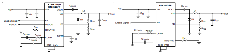
RT6362 Simplified Application Circuit
Ordering Information
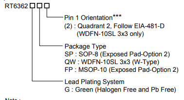
Note :
Empty means Pin1 orientation is Quadrant 1
Richtek products are :
RoHS compliant and compatible with the current requirements of IPC/JEDEC J-STD-020.
Suitable for use in SnPb or Pb-free soldering processes.
RT6362 Pin Configuration
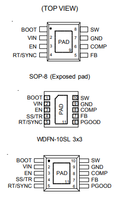
MSOP-10 (Exposed pad)
RT6362 Functional Pin Description
| Pin No. | Pin Name | Pin Function | SOP-8 (Exposed Pad) | WDFN-10SL 3x3 | MSOP-10 (Exposed Pad) |
|---|---|---|---|---|---|
| 1 | BOOT | Bootstrap capacitor connection node that supplies the high-side gate driver. Connect a 0.1µF ceramic capacitor between BOOT and SW pins. | ✓ | ✓ | ✓ |
| 2 | VIN | Power input pin. Accepts input voltages from 4V to 60V. Connect an appropriate input capacitor between VIN and GND — typically two 2.2µF or larger ceramic capacitors, with one commonly being 4.7µF. | ✓ | ✓ | ✓ |
| 3 | EN | Enable control pin with an internal pull-up current source. Leave floating or apply a logic-high (≥ 1.25V) to enable the converter. Pulling it low places the device in shutdown mode. | ✓ | ✓ | ✓ |
| – | SS/TR | Soft-start and tracking control input. Connect a capacitor from SS/TR to GND to set the soft-start period. Do not leave this pin floating, as it may cause inrush current at startup. This pin can also be used for voltage tracking or sequencing since its voltage can override the internal reference. | – | ✓ | ✓ |
| 4 | RT/SYNC | Switching frequency adjustment and synchronization input. Connect a resistor from this pin to GND to set the switching frequency. It can also be tied to an external clock source for frequency synchronization. | ✓ | ✓ | ✓ |
| – | PGOOD | Open-drain power-good output. After startup, PGOOD is pulled low to GND whenever any internal protection function is activated. | – | ✓ | ✓ |
| 5 | FB | Feedback input for output voltage sensing. Connect a resistor divider from the output to FB to set the output voltage. The typical feedback reference voltage is 0.8V. | ✓ | ✓ | ✓ |
| 6 | COMP | Compensation node. Connect external compensation components to stabilize the control loop. | ✓ | ✓ | ✓ |
| 7 | GND | Ground pin. Serves as the return path for all control circuitry. | ✓ | ✓ | ✓ |
| 8 | SW | Switch node. This pin delivers power to the output. Connect the output LC filter between SW and the load. | ✓ | ✓ | ✓ |
| 9 (Exposed Pad) | PAD | Exposed thermal pad. Internally isolated, it should be soldered to a large copper area on the PCB for optimal heat dissipation. | ✓ | ✓ | ✓ |
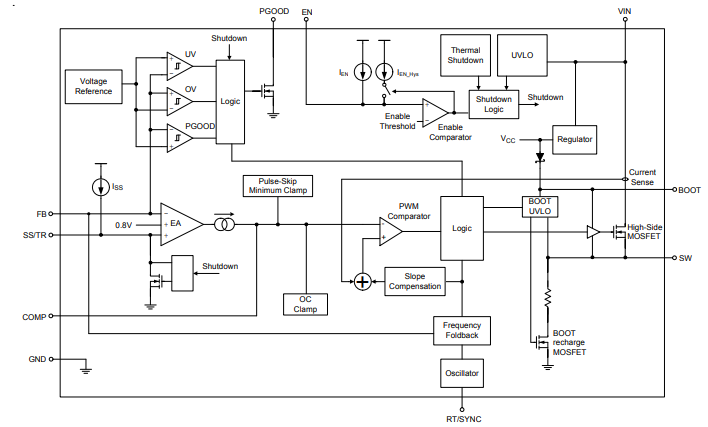
RT6362 Functional Block Diagram
WDFN-10SL 3x3 and MSOP-10 (Exposed pad) package
RT6362 Functional Block Diagram
SOP-8 (Exposed pad) package
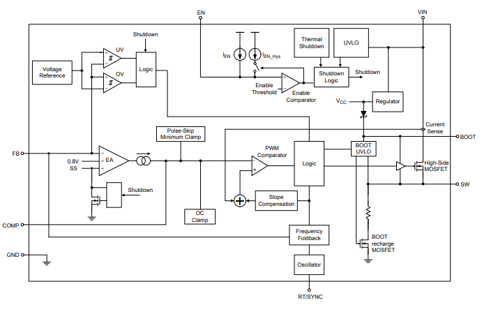
SOP-8 (Exposed pad) package
Operation
Control Loop
The RT6362 is a high-efficiency asynchronous step-down converter that uses peak current mode control.
An internal oscillator initiates each switching cycle by turning on the high-side MOSFET. At the beginning of each cycle, the MOSFET conducts, allowing the inductor current to ramp up.
The inductor current is continuously monitored during each switching cycle. The output voltage, sensed through a resistor divider (R1 and R2) connected to the FB pin, is compared to the internal reference voltage (VREF) to produce a compensation signal (VCOMP) on the COMP pin.
The converter compares the signal derived from the inductor current with the COMP voltage (generated from the feedback loop). When the inductor current reaches its threshold level, the high-side MOSFET turns off, and the inductor current flows through the external freewheeling diode connected between the SW and GND pins.
This process repeats every clock cycle, regulating both the duty cycle and output voltage by controlling the inductor current.
Light Load Operation
To improve efficiency at light loads, the RT6362 automatically enters Power Saving Mode (PSM).
In this mode, switching begins when the feedback voltage (VFB) drops below the PSM threshold (typically VREF × 1.005) and stops when VFB rises above it.
During PSM, the converter limits the inductor peak current (IL_PEAK) by clamping the COMP voltage. During non-switching intervals, most internal circuits are powered down, reducing the supply current to its quiescent level (typically 90μA) to minimize power loss.
As the load decreases, non-switching intervals become longer, effectively lowering the switching frequency and reducing both switching and gate-drive losses.
Switching Frequency Selection and Synchronization
The RT6362 provides an RT/SYNC pin for setting or synchronizing the switching frequency.
By connecting a resistor (RRT/SYNC) between the RT/SYNC pin and GND, the frequency can be adjusted within a range of 100kHz to 2.5MHz.
The device can also synchronize to an external clock source ranging from 300kHz to 2.2MHz via the same pin. The synchronization frequency must be equal to or higher than the internally set frequency.
For example, if synchronization is desired at 500kHz, select RRT/SYNC for a corresponding 500kHz internal setting.
The RT6362 also includes a frequency foldback function for protection under overload or short-circuit conditions—particularly at higher switching frequencies and input voltages.
When the feedback voltage (VFB) drops from 0.8V to 0V, the switching frequency is automatically reduced (divided by 1, 2, 4, or 8) to allow more time for the inductor current to ramp down safely. This foldback behavior applies in both resistor-set and synchronization modes.
Maximum Duty Cycle Operation
The RT6362 is designed to operate in dropout mode, achieving a maximum duty cycle approaching 100%.
When the required off-time becomes shorter than the minimum allowable off-time, the converter automatically activates a skip off-time function, keeping the high-side MOSFET continuously on to maintain output regulation.
This feature ensures the output voltage remains close to the input voltage even when the input momentarily drops near the desired output level.
The point at which the device enters dropout depends on several factors — including input and output voltage, switching frequency, load current, and overall efficiency.
The minimum input voltage required for normal operation can be estimated using the following equation:VIN_MIN=VOUT+IOUT_MAX×RL+VD1−fSW×tOFF_MIN+IOUT_MAX×RDS(ON)_H+VDV_{IN\_MIN} = \frac{V_{OUT} + I_{OUT\_MAX} \times R_L + V_D}{1 - f_{SW} \times t_{OFF\_MIN}} + I_{OUT\_MAX} \times R_{DS(ON)\_H} + V_DVIN_MIN=1−fSW×tOFF_MINVOUT+IOUT_MAX×RL+VD+IOUT_MAX×RDS(ON)_H+VD
Where:
- VIN_MINV_{IN\_MIN}VIN_MIN: Minimum input voltage for normal operation
- RDS(ON)_HR_{DS(ON)\_H}RDS(ON)_H: On-resistance of the high-side MOSFET
- VDV_DVD: Forward voltage of the freewheeling diode
- RLR_LRL: DC resistance of the inductor
- fSWf_{SW}fSW: Switching frequency
- tOFF_MINt_{OFF\_MIN}tOFF_MIN: Minimum off-time
BOOT UVLO (Bootstrap Under-Voltage Lockout)
The BOOT UVLO circuit ensures that the voltage across the bootstrap capacitor remains sufficient to properly drive the high-side MOSFET under all operating conditions.
This function typically becomes active under conditions with an extremely high step-down ratio or during light-load operation at higher output voltages.
When the voltage between BOOT and SW drops below the BOOT UVLO lower threshold (VBOOT_UVLO_L, typically 2.7V), the device automatically turns on the internal bootstrap recharge FET (typically for 150ns) to recharge the bootstrap capacitor.
The BOOT UVLO condition is cleared once the BOOT-to-SW voltage exceeds the upper threshold (VBOOT_UVLO_H, typically 2.8V).
Enable Control
The RT6362 features an EN (Enable) pin that allows external control of the device’s on/off state.
When the EN voltage (VEN) is below the enable threshold, switching is disabled — even if VIN is above the input UVLO rising threshold (VUVLOH).
If VEN falls below 0.4V, the converter enters shutdown mode, reducing the supply current to approximately 1.3μA (typical).
When VEN rises above the enable threshold and VIN exceeds VUVLOH, the device turns on, initiating switching and the soft-start sequence.
The EN pin includes an internal pull-up current source (IEN, typically 0.9μA), allowing the RT6362 to automatically enable when the pin is left floating.
The EN pin can also be used to adjust the UVLO threshold and hysteresis using two external resistors.
To implement hysteresis control, the RT6362 includes an additional hysteresis current source (IEN_Hys, typically 2.9μA), which is sourced from the EN pin when VEN is higher than the enable threshold. This hysteresis current stops once VEN falls below the enable threshold, effectively defining the turn-on and turn-off behavior.
Soft-Start and Tracking Control
The soft-start (SS) function limits the inrush current during power-up by gradually increasing the output voltage.
Different RT6362 versions provide different implementations:
- RT6362GSP: Internal soft-start
- RT6362GQW / RT6362GFP: External soft-start and tracking via the SS/TR pin
For devices with an SS/TR pin, the soft-start time can be programmed by connecting an external capacitor (CSS/TR) between SS/TR and GND, or by applying an external ramp voltage to the SS/TR pin.
During startup, the internal soft-start current source (ISS, typically 2μA) charges the external capacitor, generating a ramp voltage that serves as the reference input for the PWM comparator.
Switching begins once the voltage difference between SS/TR and FB reaches 75mV (i.e., VSS/TR − VFB = 75mV, typical).
If the output is pre-biased to a certain voltage before startup, the converter will wait until the SS/TR voltage exceeds the feedback voltage by 75mV before switching resumes. During this period, VFB tracks the rising SS/TR voltage with the same 75mV offset, ensuring a smooth and monotonic ramp-up of the output voltage.
Note: The SS/TR pin must never be left floating, as this may cause uncontrolled startup behavior.
Once the FB voltage rises above 94% of VREF (typical), the PGOOD pin transitions to a high-impedance state, and VPGOOD is pulled high to indicate that the output is within regulation.
The typical startup waveform (as shown in Figure 1) illustrates the timing relationship between the output voltage, soft-start ramp, and related control signals.
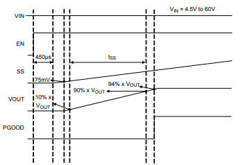
Figure 1 Start-Up Sequence for RT6362GQW and RT6362GFP
Power Good Indication
The RT6362GQW and RT6362GFP include an open-drain Power Good (PGOOD) output used to monitor the output voltage condition. A built-in comparator delay prevents false triggering of the PGOOD signal during brief output voltage fluctuations caused by line or load transients.
The PGOOD pin should be connected to an external voltage source through a pull-up resistor. It is recommended to use a resistor between 1 kΩ and 10 kΩ to minimize switching noise coupling into the PGOOD pin. The PGOOD function becomes active when the input voltage rises above 1.5 V.
This function operates through a comparator linked to the feedback voltage (VFB). When VFB increases above the Power-Good High Threshold (VTH_PGLH1) — typically 94% of the reference voltage — the PGOOD pin switches to high impedance, allowing VPGOOD to be pulled high after a short delay.
If VFB drops below the Power-Good Low Threshold (VTH_PGHL2) — typically 92% of the reference voltage — or rises above VTH_PGHL1 (109% of the reference voltage), the PGOOD pin will be pulled low. When VFB returns to within the normal range and falls below VTH_PGLH2 (106% of the reference voltage), VPGOOD is released and returns high.
After startup, if any internal protection is triggered, the PGOOD signal will also be pulled low to ground. This is achieved through an internal open-drain pull-down device with a typical resistance of 6 Ω.
The relationship between output voltage and the PGOOD signal is illustrated in Figure 2.
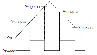
Figure 2. The Logic of PGOOD for RT6362GQW and RT6362GFP
Protection Features
Input Under-Voltage Lockout (UVLO)
In addition to the EN pin, the RT6362 also supports enable control through the VIN pin. If the EN voltage (VEN) rises above the enable threshold (VTH_EN) before the input voltage (VIN) reaches the UVLO rising threshold (VUVLOH), switching is disabled until VIN exceeds VUVLOH.
This ensures the internal regulator is fully ready and prevents operation with a partially enhanced high-side MOSFET.
After startup, if VIN drops below the UVLO falling threshold (VUVLOL), the device stops switching. Once VIN rises again above VUVLOH, normal switching operation resumes.
Note that VIN = 4V is intended only for brief drops near the UVLO threshold; under normal operation, the input voltage should remain higher than VUVLOH.
High-Side MOSFET Peak Current Limit Protection
The RT6362 provides cycle-by-cycle current limit protection for the high-side MOSFET. This protection prevents damage caused by excessive inductor current — even beyond the inductor’s saturation current rating.
The controller senses the inductor current after a short delay each time the high-side MOSFET turns on. If an over-current condition is detected, the device immediately turns off the MOSFET, limiting the peak current to the high-side current limit (ILIM).
Output Under-Voltage Protection (UVP)
To protect against overload or short-circuit conditions, the RT6362 continuously monitors the feedback voltage (VFB).
If VFB falls below 50% of the reference voltage, the UV comparator triggers, turning off the internal high-side switch.
If the under-voltage condition persists, the device enters hiccup mode. In this mode, the soft-start capacitor CSS/TR is discharged by an internal current source (ISS_DIS = 0.5 µA, typical).
The converter remains shut down until the SS voltage drops below 54 mV, after which it automatically attempts to restart. During restart, an internal charging current source (ISS = 2 µA) gradually recharges the soft-start capacitor.
The high-side MOSFET resumes switching when the voltage difference between VSS and VFB equals 75 mV (typical).
If the under-voltage fault persists, switching stops again when VSS – VFB = 1.2 V, and the discharge cycle repeats.
This auto-recovery process continues until the fault is cleared, allowing the device to protect itself with low input current and power dissipation.
A short-circuit protection and recovery behavior is illustrated in Figure 3.
The soft-start discharge time (tSS_DIS1) can be estimated using:tSS_DIS1=VSS×CSSISS_DISt_{SS\_DIS1} = \frac{V_{SS} \times C_{SS}}{I_{SS\_DIS}}tSS_DIS1=ISS_DISVSS×CSS
In short-circuit conditions (VFB ≈ 0), the following equations can be used to calculate the discharge and charge times of CSS/TR:tSS_DIS2=1.146×CSSISS_DIS,tSS_CH=1.146×CSSISSt_{SS\_DIS2} = 1.146 \times \frac{C_{SS}}{I_{SS\_DIS}}, \quad t_{SS\_CH} = 1.146 \times \frac{C_{SS}}{I_{SS}}tSS_DIS2=1.146×ISS_DISCSS,tSS_CH=1.146×ISSCSS
Output Over-Voltage Protection (OVP)
The RT6362 also includes an output over-voltage protection circuit to prevent excessive output voltage.
During overload or short-circuit events, VFB falls below VREF, causing the COMP voltage to rise and demand maximum output current. Once the fault is removed, COMP returns to its normal level to regulate the output.
However, if the load changes faster than the compensation loop can respond, an output overshoot may occur, particularly with small output capacitance.
If VFB exceeds 109% of VREF, the high-side MOSFET is forced off to limit output voltage.
When VFB falls back below 106% of VREF, switching resumes.
Over-Temperature Protection (OTP)
The RT6362 includes an over-temperature protection circuit to safeguard the IC from thermal damage caused by excessive power dissipation.
When the junction temperature exceeds the shutdown threshold (TSD), switching stops immediately.
Once the temperature drops below TSD by a hysteresis margin (ΔTSD), the device automatically restarts with a complete soft-start cycle.
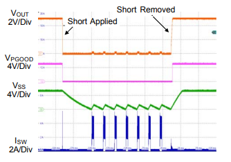
Figure 3. Short Circuit Protection and Recovery
Conclusion
The RT6362 integrates comprehensive protection features to ensure safe and reliable operation under various fault conditions. Its UVLO and enable control guarantee stable startup, while the high-side current limit, under-voltage, and over-voltage protections safeguard against overloads and short circuits. The built-in hiccup mode and thermal shutdown further enhance system safety by reducing power dissipation during faults and allowing automatic recovery once normal conditions return. Together, these protection mechanisms provide robust performance and long-term reliability for power management applications.

Christopher Anderson
Christopher Anderson has a Ph.D. in electrical engineering, focusing on power electronics. He’s been a Senior member of the IEEE Power Electronics Society since 2021. Right now, he works with the KPR Institute of Engineering and Technology in the U.S. He also writes detailed, top-notch articles about power electronics for business-to-business electronics platforms.
Subscribe to JMBom Electronics !


