


NE1618 Dual-Channel Temperature Monitor IC – Complete Overview
Catalog
DESCRIPTIONFEATURESAPPLICATIONSNE1618 PIN CONFIGURATIONNE1618 FUNCTIONAL BLOCK DIAGRAMNE1618 TYPICAL OPERATING CIRCUITELECTRICAL CHARACTERISTICSFUNCTIONAL DESCRIPTIONConclusionDESCRIPTION
The NE1618 is a high-precision, dual-channel temperature monitoring device. It measures both its own temperature and that of an external (remote) sensor. When operating in extended mode, it can serve as a direct replacement for the NE1617, providing improved accuracy in remote temperature measurements.
NE1618 Dual-Channel Temperature Monitor IC
The remote sensor can be a diode-connected transistor, either a discrete NPN/PNP type such as the 2N3904/2N3906, or a diode-connected PNP integrated within another chip, as found in some Intel® microprocessors.
Temperature readings from both the local and remote sensors are stored in internal registers and can be accessed via a 2-wire SMBus interface. These readings are automatically updated at the end of each conversion cycle when conversions are enabled. The conversion process runs automatically at a rate defined by the programmable data in the conversion rate register, although a conversion can also be triggered immediately using the one-shot mode.
The local temperature is always measured with a 1.0 °C resolution, while the remote sensor offers two selectable measurement modes:
- Extended mode: 0.125 °C resolution
- Basic mode: 1.0 °C resolution
The operating mode is automatically selected based on the data stored in the conversion rate register (see Table 6). Extended mode is used when the conversion rate is low (0.7 Hz or less), while normal mode applies at higher rates (2, 4, or 8 Hz).
An integrated temperature alarm detects both over-temperature and under-temperature conditions, with programmable trip points. The NE1618 supports nine possible SMBus addresses (determined by two address pins), allowing up to nine devices to be connected on the same bus.
For power efficiency, the device can enter standby mode, which can be activated either through software (via the SMBus) or hardware (using the STBY pin).
FEATURES
• Monitors both local and remote temperatures
• High measurement accuracy:
– ±2 °C for local (on-chip) sensor
– ±1.5 °C for remote sensor at 1 °C resolution
– ±1.0 °C for remote sensor at 0.125 °C resolution
• No external calibration required
• Programmable over- and under-temperature alarm
• SMBus-compatible 2-wire serial interface
• Operates from 3.0 V to 3.6 V supply
• Low power consumption:
– 80 µA (operating mode)
– 3 µA typical (standby mode)
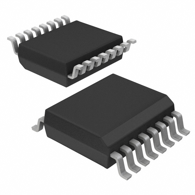
• Compact 16-lead QSOP package
APPLICATIONS
• Desktop PCs
• Laptop and notebook computers
• Smart battery packs
• Industrial control systems
• Telecommunications equipment
NE1618 PIN CONFIGURATION
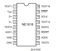
NE1618 PIN DESCRIPTION
| Pin # | Function | Description / Comments |
|---|---|---|
| 1 | TEST1 | Reserved for factory testing¹ |
| 2 | VDD | Positive power supply² |
| 3 | D+ | Positive input of the remote temperature sensor |
| 4 | D– | Negative input of the remote temperature sensor |
| 5 | TEST5 | Reserved for factory testing¹ |
| 6 | ADD1 | Device address selection pin (3-state) |
| 7 | GND | Ground |
| 8 | GND | Ground |
| 9 | TEST9 | Reserved for factory testing¹ |
| 10 | ADD0 | Device address selection pin (3-state) |
| 11 | ALERT | Open-drain output for interrupt or SMBus alert function |
| 12 | SDATA | SMBus serial data input/output (open-drain) |
| 13 | TEST13 | Reserved for factory testing¹ |
| 14 | SCLK | SMBus clock input |
| 15 | STBY | Hardware standby control pin — HIGH: normal operation, LOW: standby mode |
| 16 | TEST16 | Reserved for factory testing¹ |
NOTES:
- Factory test pins should remain floating or connected to ground.
- The VDD pin should be decoupled with a 0.1 µF capacitor for stable operation.
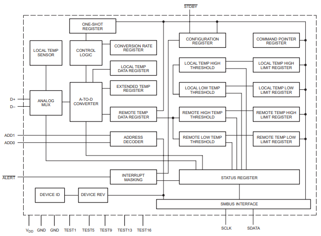
NE1618 FUNCTIONAL BLOCK DIAGRAM
NE1618 TYPICAL OPERATING CIRCUIT
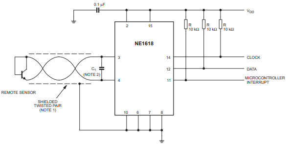
NOTES:
1. May be required if remote diode is in a noisy environment and/or several feet from the NE1618.
2. May be required in noisy environment. Up to 2200 pF may be used.
ABSOLUTE MAXIMUM RATINGS
| Parameter | Min. | Max. | Unit |
|---|---|---|---|
| VDD to GND | –0.3 | +6 | V |
| D+, ADD0, ADD1 | –0.3 | VDD + 0.3 | V |
| D– to GND | –0.3 | +0.8 | V |
| SCLK, SDATA, ALERT, STBY | –0.3 | +6 | V |
| Input current (SDATA) | –1 | +50 | mA |
| D– current | — | ±1 | mA |
| ESD – Human Body Model | — | 2000 | V |
| ESD – Machine Model | — | 200 | V |
| Operating temperature range | 0 | +120 | °C |
| Maximum junction temperature | — | +150 | °C |
| Storage temperature range | –65 | +150 | °C |
NOTE:
- These are stress ratings only. Functional operation of the device under these or any conditions beyond those described in the operational specifications is not guaranteed. Exposure to absolute maximum conditions for extended periods may result in permanent damage and affect long-term reliability.
ELECTRICAL CHARACTERISTICS
(VDD = 3.3 V; Tamb = +5 °C to +120 °C, unless otherwise specified)
| Parameter | Conditions | Min. | Typ. | Max. | Unit |
|---|---|---|---|---|---|
| Temperature resolution | — | — | 1 | — | °C |
| Local temperature error | Tamb = +60 °C to +100 °C, VDD = 3.3 V | — | ±0.75 | ±1.5 | °C |
| Tamb = +60 °C to +100 °C, VDD = 5.0 V¹ | — | ±1.25 | ±2.0 | °C | |
| Tamb = 0 °C to +120 °C, VDD = 3.3 V | — | ±2.0 | ±3.0 | °C | |
| Tamb = 0 °C to +120 °C, VDD = 5.0 V¹ | — | ±2.5 | ±3.5 | °C | |
| Remote temperature error (1 °C resolution) | Tremote = +60 °C to +100 °C, VDD = 3.3 V | — | — | ±3.0 | °C |
| Tremote = +60 °C to +100 °C, VDD = 5.0 V¹ | — | — | ±3.5 | °C | |
| Tremote = 0 °C to +120 °C, VDD = 3.3 V | — | — | ±5.0 | °C | |
| Tremote = 0 °C to +120 °C, VDD = 5.0 V¹ | — | — | ±5.5 | °C | |
| Extended remote temperature error (0.125 °C resolution) | Tremote = +70 °C to +100 °C, VDD = 3.3 V | — | — | ±1.0 | °C |
| Tremote = +70 °C to +100 °C, VDD = 5.0 V¹ | — | — | ±1.5 | °C | |
| Tremote = 0 °C to +120 °C, VDD = 3.3 V | — | — | ±3.0 | °C | |
| Tremote = 0 °C to +120 °C, VDD = 5.0 V¹ | — | — | ±3.5 | °C | |
| Extended relative temperature error (0.125 °C resolution) | Tremote = +70 °C to +100 °C, VDD = 3.3 V | — | ±0.25 | — | °C |
| Tremote = +70 °C to +100 °C, VDD = 5.0 V¹ | — | ±0.75 | — | °C | |
| Tremote = 0 °C to +120 °C, VDD = 3.3 V | — | ±0.50 | — | °C | |
| Tremote = 0 °C to +120 °C, VDD = 5.0 V¹ | — | ±1.0 | — | °C | |
| Under-voltage lockout³ | VDD input disables A/D conversion⁴ | 2.1 | — | 2.95 | V |
| Power-on reset threshold⁵ | VDD input falling edge | 1.0 | — | 2.5 | V |
| Power supply current (average) | Conversion rate = 02h | 80 | — | 160 | µA |
| Conversion rate = 05h | 100 | — | 270 | µA | |
| Power supply current (standby) | SMBus inactive | 3 | — | 10 | µA |
| Conversion time (busy duration) | Basic measurement | — | 150 | — | ms |
| Extended measurement | — | 750 | — | ms | |
| Conversion rate error | Programmed rate > 1 Hz⁶ | –30 | — | +30 | % |
| Remote sensor source current | HIGH level | 100 | — | — | µA |
| LOW level | 10 | — | — | µA | |
| Address pin bias current | During address read⁷⁸ | — | — | 50 | µA |
NOTES:
- The NE1618 is optimized for 3.3 V operation. The accuracy limits listed for 5 V operation are guaranteed by design and verified through 100% QA sample testing.
- Guaranteed by design.
- Under-Voltage Lockout (UVL) is defined as the minimum VDD level below which the internal A/D converter is disabled. This threshold is designed to be at least 200 mV above the power-on reset voltage. While disabled, the temperature registers retain their last valid readings to prevent incorrect data due to low voltage. Upon power-up, the temperature register defaults to 0 °C until VDD rises above the UVL threshold.
- VDD (rising edge) level below which the ADC remains inactive.
- VDD (falling edge) level below which internal logic resets.
- For conversion rates ≤ 1 Hz, extended measurements require approximately 400 ms longer conversion time.
- Device address is read at power-up and at the start of each conversion (except at the fastest conversion rate).
- Due to address pin bias current, pull-up or pull-down resistors should be ≤ 2 kΩ.
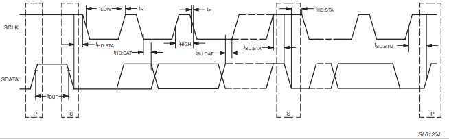
SMBus INTERFACE AC SPECIFICATIONS
(VDD = 3.0 V to 3.6 V; Tamb = 0 °C to +125 °C, unless otherwise specified)
These specifications are guaranteed by design and not tested in production.
| Symbol | Parameter | Conditions | Min. | Typ. | Max. | Unit |
|---|---|---|---|---|---|---|
| VIH | Logic input high voltage for STBY, SCLK, SDATA | VDD = 3.0 V to 5.5 V | 2.2 | — | — | V |
| VIL | Logic input low voltage for STBY, SCLK, SDATA | VDD = 3.0 V to 5.5 V | — | — | 0.8 | V |
| IOL | Logic output low sink current — ALERT | VOL = 0.4 V | 1.0 | — | — | mA |
| Logic output low sink current — SDATA | VOL = 0.6 V | — | — | 6.0 | mA | |
| IIH, IIL | Logic input current | VIN = VDD or GND | — | ±1.0 | — | µA |
| CIN | SMBus input capacitance (SCLK, SDATA) | — | — | 5 | — | pF |
| fSCLK | SCLK operating frequency | See Figure 4 | 0 | — | 100 | kHz |
| tLOW | SCLK low time | See Figure 4 | 4.0 | — | — | µs |
| tHIGH | SCLK high time | See Figure 4 | 4.0 | 5.0 | — | µs |
| tBUF | Bus free time between STOP and START condition | See Figure 4 | 4.7 | — | — | µs |
| tHD:STA | Hold time after START condition (SDA start to first SCL low) | See Figure 4 | 4.0 | — | — | µs |
| tHD:DAT | Data hold time (SCL high-to-low to SDA edge) | See Figure 4 | 0 | — | — | ns |
| tSU:DAT | Data setup time (SDA edge to SCL low) | See Figure 4 | 250 | — | — | ns |
| tSU:STA | Setup time for repeated START condition (SCL low-to-high to next START) | See Figure 4 | 250 | — | — | ns |
| tSU:STO | Setup time for STOP condition (SCL low-to-high to SDA high) | See Figure 4 | 4.0 | — | — | µs |
| tF | Fall time of SCL and SDA signals | See Figure 4 | — | — | 1.0 | µs |
Note:
Timing parameters refer to standard SMBus protocol operation. For reliable communication, ensure bus pull-up resistors are selected to maintain rise and fall times within the specified limits.
Timing measurements.
NOTE:
The NE1618 does not include the SMBus timeout capability (tLOW:SEXT and tLOW:MEXT).
FUNCTIONAL DESCRIPTION
Serial Bus Interface
The NE1618 communicates through a 2-wire System Management Bus (SMBus) interface, operating as a slave device controlled by a master controller. Communication takes place via two pins: SCLK (clock input) and SDATA (data input/output).
The master device generates the clock signal on the SCLK line and transfers data to or from the NE1618 through the SDATA line. Because both pins use open-drain circuitry, external pull-up resistors (typically around 10 kΩ) are required on each line.
All communication between the controller and the NE1618 uses 8-bit data bytes or words following standard SMBus protocol, which will be explained further in the SMBus Interface section. Detailed device operations over the bus are discussed in the following sections.
Slave Address
The 7-bit slave address of the NE1618 on the SMBus is determined by the logic levels applied to the ADD0 and ADD1 pins. Each of these pins can be configured to one of three logical states:
- Connected to GND
- Connected to VDD
- Left floating (open)
To ensure reliable address detection, any pull-up or pull-down resistors used should be ≤ 2 kΩ. The available address combinations are shown in Table 1, providing up to nine unique address options, allowing multiple NE1618 devices to operate on the same SMBus without address conflict.
It is important to note that the state of the address pins is sampled and latched both at power-up and at the start of every conversion. Therefore, the address configuration must remain permanently connected during device operation to ensure stable communication.
Registers
The NE1618 includes several internal registers whose names, commands, power-on reset (POR) states, and functions are listed in Table 2. These registers serve various purposes, such as:
- Configuration register – used to control and configure the NE1618’s operation.
- Status register – provides flag indicators resulting from temperature limit comparisons.
- Temperature measurement and limit registers – store temperature readings and limit settings.
- Identification and test registers – used for device identification and factory testing.
Each register stores data in an 8-bit digital byte format. Temperature-related data are represented in two’s complement format, while all other data use straight binary format. Registers hold either programmable values that define device behavior or measured data from internal operations.
Register access is controlled via the command byte, which specifies the target register during SMBus communication. Data read and write operations are performed by the system controller through the SMBus.
Registers are organized into two main groups:
- Read-only registers (R– prefix): Data can only be read.
- Write-only registers (W– prefix): Data can only be written (includes the one-shot register, OSHT).
Programmable values should be written to write-only registers, while measured or status data should be read from read-only registers. Any attempt to write to a read-only register or read from a write-only register will result in an invalid operation — written data will be ignored, and read data will return FFh.
Some registers exist in pairs to support both read and write operations for the same function (e.g., RC and WC for configuration).
Reserved registers are used solely for factory testing and should not be accessed in normal operation.
Device Slave Address
The NE1618 uses a 7-bit slave address on the SMBus, which is determined by the logic levels applied to the ADD0 and ADD1 pins. These pins can be connected to GND, VDD, or left not connected (NC). Each combination corresponds to a unique device address, as shown in the table below.
| ADD0 Pin | ADD1 Pin | 7-Bit Address (Binary) |
|---|---|---|
| GND | GND | 0011 000 |
| GND | NC | 0011 001 |
| GND | VDD | 0011 010 |
| NC | GND | 0101 001 |
| NC | NC | 0101 010 |
| NC | VDD | 0101 011 |
| VDD | GND | 1001 100 |
| VDD | NC | 1001 101 |
| VDD | VDD | 1001 110 |
Each of these nine address combinations allows multiple NE1618 devices to share the same SMBus without address conflicts.
Note: The ADD0 and ADD1 connections are sampled and latched both at power-up and at the start of each temperature conversion, so these connections must remain fixed during operation.
Register Assignments
The NE1618 contains multiple internal registers used for device configuration, status monitoring, and temperature measurement. Each register is identified by a command byte and initialized to a specific value after Power-On Reset (POR). The following table summarizes the register names, command codes, default states, and their functions.
| Register Name | Command Byte (Hex) | POR State (Binary) | Function / Description |
|---|---|---|---|
| RDID | FEH | N/A | Read Device ID |
| RDRV | FFH | N/A | Read Device Revision |
| RIT | 00H | 0000 0000 | Read Internal (Local) Temperature |
| RET | 01H | 0000 0000 | Read External (Remote) Temperature |
| REET | 10H | 0000 0000 | Read Extended External Temperature |
| RS | 02H | N/A | Read Status |
| RC | 03H | 0000 0000 | Read Configuration |
| RCR | 04H | 0000 0010 | Read Conversion Rate |
| RIHL | 05H | 0111 1111 | Read Internal Temperature High Limit |
| RILL | 06H | 1100 1001 | Read Internal Temperature Low Limit |
| REHL | 07H | 0111 1111 | Read External Temperature High Limit |
| RELL | 08H | 1100 1001 | Read External Temperature Low Limit |
| WC | 09H | N/A | Write Configuration |
| WCR | 0AH | N/A | Write Conversion Rate |
| WIHL | 0BH | N/A | Write Internal Temperature High Limit |
| WILL | 0CH | N/A | Write Internal Temperature Low Limit |
| WEHL | 0DH | N/A | Write External Temperature High Limit |
| WELL | 0EH | N/A | Write External Temperature Low Limit |
| OSHT | 0FH | N/A | One-Shot Command |
| RESERVED | 11H | N/A | Reserved for Factory Use |
| RESERVED | 12H | N/A | Reserved for Factory Use |
| RESERVED | 13H | N/A | Reserved for Factory Use |
| RESERVED | 14H | N/A | Reserved for Factory Use |
| RESERVED | 15H | N/A | Reserved for Factory Use |
Notes:
- Registers beginning with “R–” are read-only.
- Registers beginning with “W–” are write-only.
- Attempting to write to a read-only register or read from a write-only register results in invalid data (read value = FFh).
- The OSHT register is a one-shot command register, used to trigger a single temperature conversion.
- Reserved registers are intended for manufacturer test purposes and should not be accessed by the user.
Power-On Reset (POR)
When power is applied to the NE1618 while the STBY input pin is LOW, the device enters its Power-On Reset (POR) state, during which all registers are reset to their default values (see Table 2). The POR state results in:
- The interrupt latch is cleared, the ALERT output driver is off, and the ALERT pin is pulled HIGH via an external pull-up resistor.
- The conversion rate is set to the default value of approximately 0.2 Hz.
- Temperature limits for both local and remote channels are set to +127 °C (high limit) and –55 °C (low limit).
- The register pointer is set to 00H, ready for reading RIT (internal temperature) data.
Registers with indeterminate default values will contain unknown data after POR.
During POR, the on-board A-to-D converter is disabled, and the device’s measurement functions are inactive. However, the SMBus interface remains active, allowing read/write operations to registers. If no SMBus activity occurs, the device consumes less than 10 µA of supply current. Writing temperature limit values to the limit registers is recommended during this stage.
Starting Conversion
After POR, if the STBY pin is HIGH and the RUN/STOP bit (bit 6) of the configuration register is 0 (default), the device enters free-running mode:
- The A-to-D converter is enabled, and temperature measurement is activated.
- The device automatically cycles through local and remote temperature measurements at intervals defined by the programmable conversion rate register.
- Temperature readings are compared against limit values to update status flags and trigger interrupts via the ALERT pin.
- Measured values are stored in the temperature registers, while limit comparison results update the status register.
To prevent false status flags, temperature limit values should be written into the limit registers before starting conversion.
Low-Power Standby Modes
The NE1618 can be placed into standby mode from free-running operation in two ways:
- Hardware Standby Mode – Set the STBY pin LOW.
- Software Standby Mode – Set the RUN/STOP bit (bit 6) of the configuration register to 1.
In both modes:
- Free-running operation is halted.
- Supply current drops to less than 10 µA if there is no SMBus activity.
- All register data are retained.
- The SMBus interface remains active, so register read/write operations are still possible.
Key differences between standby modes:
- Software Standby: The A-to-D converter can still perform measurements. A one-shot command initiates a single conversion, which updates temperature registers and status flags as in free-running mode.
- Hardware Standby: The A-to-D converter is fully disabled. Conversion operations are inhibited, and no measurements are performed. If a hardware standby command is received during an ongoing conversion, the cycle is stopped immediately, and temperature registers are not updated.
Temperature Measurement
The NE1618 features an on-chip sensor for measuring the local (internal) temperature and provides two input pins, D+ and D–, for connecting an external (remote) temperature sensor. The remote sensor must be a diode-type device, connected with the anode to D+ and cathode to D–.
Measurement Principle
Temperature is determined by measuring the base-emitter voltage difference (ΔVBE) of the diode at two different operating currents:ΔVBE=kTqln(N)\Delta V_{BE} = \frac{kT}{q} \ln(N)ΔVBE=qkTln(N)
Where:
- k = Boltzmann’s constant
- T = Absolute temperature (Kelvin)
- q = Electron charge
- LN = Natural logarithm
- N = Ratio of the two current levels
For remote temperature measurement, the NE1618 provides two current sources (~10 µA and ~100 µA). The sensed voltage across D+ and D– is limited to 0.25 V – 0.95 V, so the external diode must operate within these current and voltage limits. Recommended devices include:
- PNP transistor diode-connected on Intel Pentium microprocessors
- Discrete low-power transistor, e.g., 2N3904
Conversion to Digital Data
The ΔVBE voltage is converted to a digital value using the on-chip sigma-delta A-to-D converter. The results are:
- Stored in the temperature registers: RIT (local), RET (remote), and REET (extended remote).
- Compared against temperature limits to update the status register flags and trigger an ALERT interrupt if any limit is exceeded.
Data registers are updated at the end of each conversion and can be read at any time.
Measurement Modes
- Basic Measurement: Resolution: 1 °C for local and remote sensors. Used for general-purpose temperature monitoring.
- Extended Measurement (Remote Only): Resolution: 0.125 °C, enabled for precise monitoring (e.g., IC die temperature). Uses the 11-bit A-to-D converter: 8 MSB bits → RET register 3 LSB bits → REET register (stored in MSB positions) To obtain the extended remote temperature, combine RET and REET data correctly.
In basic mode (conversion rate > 04h), only the RET register is significant; REET is cleared, and resolution is 1 °C.
The extended measurement works only in free-running mode. One-shot conversions or standby operations produce basic measurement results regardless of conversion rate settings.
Temperature Data Format
- Local Temperature (RIT): Measured in integer values, 1 °C resolution. Represented in 2’s complement 8-bit format.
- Remote Temperature (RET + REET): Measured as a floating-point value, consisting of: Integer portion from RET (Table 3) Fractional/extended portion from REET (Table 4) In basic measurement mode, the extended portion = 0; the temperature is derived solely from RET.
Table 3. Temperature Data Format (RIT & RET)
The RIT (local temperature) and RET (remote temperature) registers store temperature values in 8-bit digital 2’s complement format with 1 °C resolution.
| Temperature (°C) | 8-Bit Digital Data |
|---|---|
| +127 | 0111 1111 |
| +126 | 0111 1110 |
| +100 | 0110 0100 |
| +50 | 0011 0010 |
| +25 | 0001 1001 |
| +1 | 0000 0001 |
| ≤0 | 0000 0000 |
Note: Negative temperatures are represented using standard 2’s complement notation.
Conversion Rate Control Byte
The conversion rate control byte defines the temperature measurement frequency and the typical supply current at VDD = 3.3 V. Only values 00h to 07h are valid; other values (08h to FFh) are reserved.
| Data | Conversion Rate (Hz) | Average Supply Current (µA Typ.) |
| 00h | 0.06 | TBD |
| 01h | 0.12 | TBD |
| 02h | 0.22 | TBD |
| 03h | 0.40 | TBD |
| 04h | 0.70 | TBD |
| 05h | 2 | TBD |
| 06h | 4 | TBD |
| 07h | 8 | TBD |
| 08h–FFh | Reserved | n/a |
The conversion rate is used to control basic or extended measurement modes for remote temperature.
Temperature Limit Registers
The NE1618 provides four programmable temperature limit registers:
•High and low limits for internal (local) temperature
•High and low limits for external (remote) temperature
Function:
•Each channel’s measured temperature (RIT for local, RET for remote) is compared with its corresponding limit register.
•If the temperature equals or exceeds the limit: The ALERT output is asserted The corresponding status flag bit is set
Commands:
| Register | Function |
| WIHL / RIHL | Internal temperature high limit |
| WILL / RILL | Internal temperature low limit |
| WEHL / REHL | External temperature high limit |
| WELL / RELL | External temperature low limit |
POR Default Values:
•High limit: +127 °C (0111 1111)
•Low limit: –55 °C (1100 1001)
Note: Only RET data is used for external temperature limit comparisons. The REET register is ignored.
One-Shot Command
The one-shot command (OSHT, 0Fh) is not a data register, but writing to it initiates a single ADC conversion.
•In free-running mode, a one-shot command immediately starts a new conversion cycle.
•If a conversion is already in progress, the command is ignored.
•In software standby mode, the command performs one conversion and then returns the device to standby.
•In hardware standby mode, the one-shot command is inhibited.
Important Notes:
•Using a one-shot command clears the REET register.
•The resulting measurement is always a basic measurement (1 °C resolution) regardless of extended mode settings.
Conclusion
The NE1618 is a high-precision, dual-channel temperature monitoring IC designed for accurate measurement of both local and remote temperatures. It supports basic and extended measurement modes, programmable temperature limits, and SMBus communication for easy integration into computer, industrial, and telecom systems. The device provides built-in fault detection, ALERT interrupt signaling, and low-power standby modes, ensuring reliable operation under varying conditions. Careful PCB layout, proper sensor connection, and appropriate bypassing are essential to minimize noise and maximize measurement accuracy. Overall, the NE1618 offers a versatile and robust solution for temperature monitoring in high-performance electronic applications.

Christopher Anderson
Christopher Anderson has a Ph.D. in electrical engineering, focusing on power electronics. He’s been a Senior member of the IEEE Power Electronics Society since 2021. Right now, he works with the KPR Institute of Engineering and Technology in the U.S. He also writes detailed, top-notch articles about power electronics for business-to-business electronics platforms.
Subscribe to JMBom Electronics !


