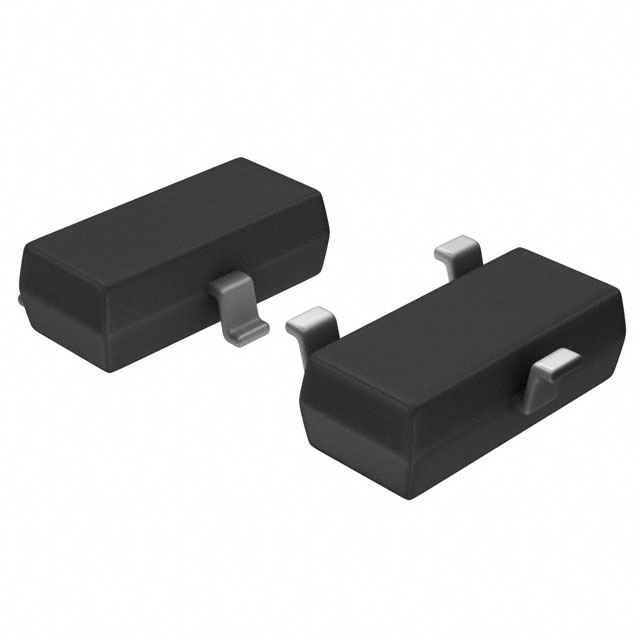
Honeywell 2455R 00870247


- Part Number:
2455R 00870247
- Manufacturer:
- Category:
- RoHs:
 Non-RoHS Compliant
 - Datasheet:
- Description:
THERMOSTAT COMMERCIAL
- In stock 0

CSD87334Q3DT Product Information Summary
Product Overview
- Manufacturer: Texas Instruments
- Model: CSD87334Q3DT
- Description: Synchronous Buck NexFET™ Power Block
Features
- Half-Bridge Power Block
- Optimized for High-Duty Cycle
- Up to 24 Vin
- 96.1% System Efficiency at 12 A
- 1.6-W PLoss at 12 A
- Up to 20-A Operation
- High-Frequency Operation (up to 1.5 MHz)
- High-Density SON 3.3 mm × 3.3 mm Footprint
- Optimized for 5-V Gate Drive
- Low-Switching Losses
- Ultra-Low-Inductance Package
- RoHS Compliant
- Halogen-Free
- Lead-Free Terminal Plating
Applications
- Synchronous Buck Converters – High-Frequency Applications
- Synchronous Boost Converters
- POL DC-DC Converters
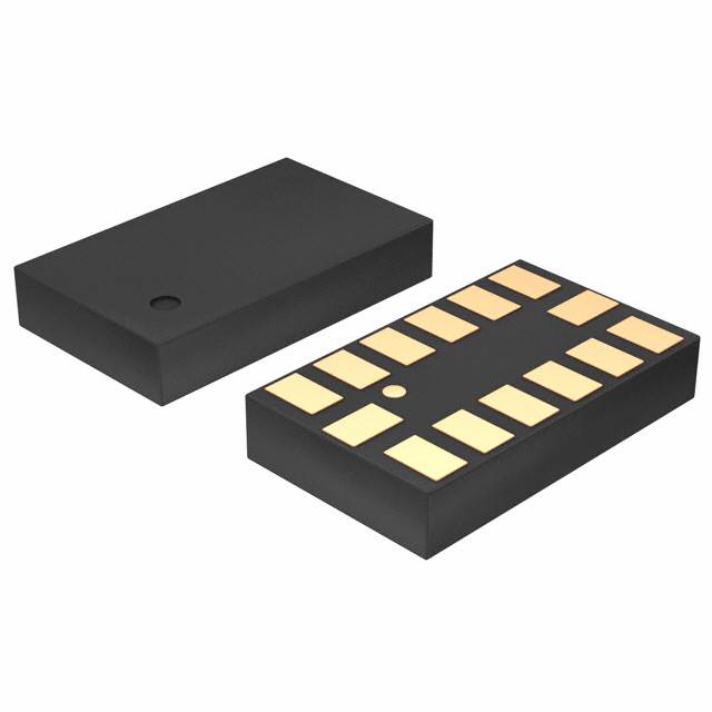
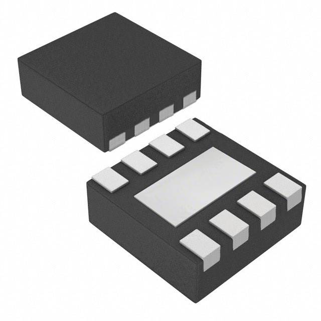
Ordering Information
- Global Part Number: CSD87334Q3DT
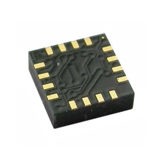
- Package: VSON-CLIP (DPB)
- Pins: 8
- Package Quantity: 250
- Carrier: SMALL T&R
- RoHS Compliant: Yes
- Lead Finish/Ball Material: NIPDAU
- MSL Rating/Peak Reflow: Level-1-260C-UNLIM
- Operating Temperature Range: -55°C to 150°C
- Part Marking: 87334D
Electrical Characteristics
- Capacitance Range: 2 pF to 1.5 nF
- Tolerance: ±10% (K)
- Temperature Coefficient: NP0 (±30 ppm/°C)
- Operating Temperature Range: -55°C to +125°C
- Safety Certification: X1/Y2 & X2/Y3
- Packaging: Tape & Reel
- Termination: Nickel-barrier end termination
- RoHS Compliant: Yes
- Halogen Free Compliant: Yes
Dimensions
- Length (L1): 4.8 mm ±0.30 mm
- Width (W): 3.2 mm ±0.30 mm
- Thickness (T): 2.0 mm ±0.20 mm
- Termination Length (L2/L3): Min 0.25 mm, Max 0.75 mm
Absolute Maximum Ratings
- VIN to PGND: 30 V
- VSW to PGND: 30 V
- TG to TGR: -0.3 V to 10 V
- BG to PGND: -0.3 V to 10 V
- IDM Pulsed current rating: 60 A
- PD Power dissipation: 6 W
- EAS Avalanche energy: 48 mJ
- TJ Operating junction temperature: -55°C to 150°C
- Tstg Storage temperature: -55°C to 150°C
Recommended Operating Conditions
- VGS Gate drive voltage: 3.3 V to 8 V
- VIN Input supply voltage: 24 V
- Switching frequency: 1500 kHz
- Operating current: 20 A
- TJ Operating temperature: 125°C
Power Block Performance
- Power Loss: 1.6 W at 12 A, 500 kHz, 3.3 V output
- VIN Quiescent Current: 10 µA
Thermal Information
- RθJA Junction-to-ambient thermal resistance: 130°C/W (min Cu), 75°C/W (max Cu)
- RθJC Junction-to-case thermal resistance: 21°C/W (top of package), 2.1°C/W (PGND pin)
Electrical Characteristics
- BVDSS Drain-to-source voltage: 30 V
- IDSS Drain-to-source leakage current: 1 µA
- IGSS Gate-to-source leakage current: 100 nA
- VGS(th) Gate-to-source threshold voltage: 0.75 V to 1.20 V
- RDS(on) Drain-to-source on resistance: 6.3 mΩ to 8.3 mΩ at 3.5 V, 5.6 mΩ to 7.0 mΩ at 4.5 V, 4.9 mΩ to 6.0 mΩ at 8 V
Typical Power Block Device Characteristics
- Power Loss vs Output Current: See Figure 1
- Power Loss vs Temperature: See Figure 2
- Safe Operating Area: See Figures 3 to 5
- Normalized Power Loss vs Switching Frequency: See Figure 6
- Normalized Power Loss vs Input Voltage: See Figure 7
- Normalized Power Loss vs Output Voltage: See Figure 8
- Normalized Power Loss vs Output Inductance: See Figure 9
Layout Guidelines
- PCB Design: Optimize for electrical and thermal performance
- Input Capacitors: Place close to VIN and PGND pins
- Driver IC: Place close to TG and BG pins
- Output Inductor: Place close to VSW pins
- Thermal Vias: Use to pull heat away from the device
Mechanical, Packaging, and Orderable Information
- Package Dimensions: See Figure 15
- Land Pattern Recommendation: See Figure 16
- Stencil Recommendation: See Figure 17
- Tape and Reel Information: See Section 9.4
Purchase
No need to register to order from JMBom Electronics, but signing in lets you track your order like a pro. Give it a try for a smoother shopping ride.
Means
Easy peasy! Pay your way with PayPal, Credit Card, or wire transfer in USD. We've got you covered.
RFQ(Request for Quotations)
Get the freshest prices and stock updates by asking for a quote! Our sales team will shoot you an email within a day. It's that simple.
IMPORTANT NOTICE
1. Look out for your order details in your inbox! (If it's missing, check the spam folder just in case.)
2. Our sales manager will double-check the order and keep you posted on any price or stock changes. No worries, we've got you covered.

Shipping Rate
We ship orders once a day around 5 p.m., except Sunday. Once shipped, the estimated delivery time depends on the courier company you choose, usually 5-7 working days.

Shipping Methods
We provide DHL, FedEx, UPS, EMS, SF Express, and Registered Air Mail international shipping.


Payment
You can pay the orders on the website directly or pay by wire transfer offline. We support: Paypal、VISA、Credit Card.