NXP 74LVC245APW/AUJ


- Part Number:
74LVC245APW/AUJ
- Manufacturer:
- Category:
- RoHs:
 RoHS Compliant
 - Datasheet:
 74LVC245APW/AUJ_Datesheet
 - Description:
IC TXRX NON-INVERT 3.6V 20TSSOP
- In stock 0

74LVC245APW/AUJ Product Information
General Description
The 74LVC245A is an 8-bit transceiver with 3-state outputs, designed for high-speed data transmission and interfacing between different voltage levels. It features an output enable (OE) and direction control (DIR) for flexible data flow management. This device is ideal for translating between 3.3V and 5V systems, ensuring reliable communication in mixed-voltage applications.
Key Features
- Wide Supply Voltage Range: 1.2V to 3.6V
- CMOS Low-Power Consumption: Suitable for low-power applications
- Direct Interface with TTL Levels: Ensures compatibility with a wide range of digital systems
- Overvoltage Tolerant Inputs: Up to 5.5V, providing robustness against voltage spikes
- Bus Hold on All Data Inputs: (74LVCH245A only) Maintains data integrity
- IOFF Circuitry: Provides partial power-down mode operation, preventing backflow current
- Compliance with JEDEC Standards: Ensures industry-standard performance and reliability
- ESD Protection: HBM exceeds 2000V, CDM exceeds 1000V, ensuring robustness against electrostatic discharge
Ordering Information
74LVC245APW
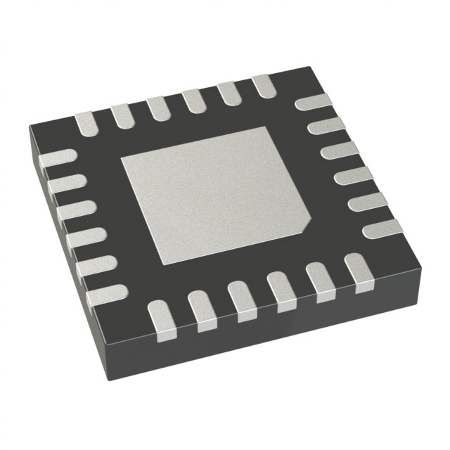
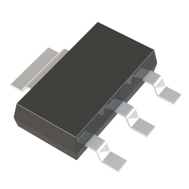
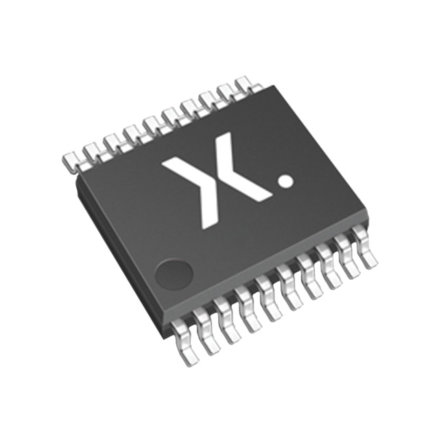
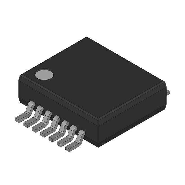
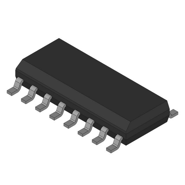
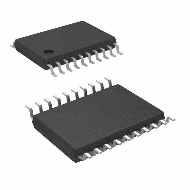
- Package Type: TSSOP20 (Plastic Thin Shrink Small Outline Package)
- Temperature Range: -40°C to +125°C
- Description: 20 leads, body width 4.4mm
- Version: SOT360-1
74LVC245AUJ
- Package Type: Not specified in the provided document
- Temperature Range: Not specified in the provided document
- Description: Not specified in the provided document
- Version: Not specified in the provided document
Pinning Information
Pin Configuration
TableCopy
| Symbol | Pin | Description |
|---|---|---|
| DIR | 1 | Direction control |
| A0-A7 | 2-9 | Data input/output |
| GND | 10 | Ground (0V) |
| B0-B7 | 11-18 | Data input/output |
| OE | 19 | Output enable input (active LOW) |
| Vcc | 20 | Supply voltage |
Functional Description
The 74LVC245A operates in three modes based on the OE and DIR inputs:
- Disabled Mode: When OE is HIGH, all outputs are in a high-impedance state.
- Transmit Mode: When OE is LOW and DIR is HIGH, data from A inputs are transmitted to B outputs.
- Receive Mode: When OE is LOW and DIR is LOW, data from B inputs are received at A outputs.
Limiting Values
- Supply Voltage (VCC): -0.5V to +6.5V
- Input Clamping Current (IIK): -50mA
- Input Voltage (VI): -0.5V to +6.5V
- Output Clamping Current (IOK): ±50mA
- Output Voltage (VO): -0.5V to +6.5V
- Output Current (IO): ±50mA
- Supply Current (ICC): 100mA
- Ground Current (IGND): -100mA to +100mA
- Storage Temperature (Tstg): -65°C to +150°C
- Total Power Dissipation (Ptot): 250mW to 500mW (depending on package type)
Recommended Operating Conditions
- Supply Voltage (VCC): 1.65V to 3.6V
- Input Voltage (VI): 0V to 5.5V
- Output Voltage (VO): 0V to VCC
- Ambient Temperature (Tamb): -40°C to +125°C
- Input Transition Rise and Fall Rate (Δt/ΔV): 0ns/V to 20ns/V (for VCC = 1.2V to 2.7V), 0ns/V to 10ns/V (for VCC = 2.7V to 3.6V)
Static Characteristics
- HIGH-Level Input Voltage (VIH): Varies with VCC (e.g., 0.65VCC for VCC = 1.65V to 1.95V)
- LOW-Level Input Voltage (VIL): Varies with VCC (e.g., 0.35VCC for VCC = 1.65V to 1.95V)
- HIGH-Level Output Voltage (VOH): VCC - 0.2V to VCC - 0.3V
- LOW-Level Output Voltage (VOL): 0V to 0.2V
- Input Leakage Current (II): ±0.1μA to ±20μA
- OFF-State Output Current (IOZ): ±0.1μA to ±20μA
- Power-Off Leakage Current (IOFF): 0.1μA to 40μA
- Supply Current (ICC): 5μA to 5000μA
Dynamic Characteristics
- Propagation Delay (tpd): Varies with VCC (e.g., 1.5ns to 17.0ns for VCC = 1.2V)
- Enable Time (ten): Varies with VCC (e.g., 1.9ns to 22.0ns for VCC = 1.2V)
- Disable Time (tdis): Varies with VCC (e.g., 1.0ns to 12.0ns for VCC = 1.2V)
- Output Skew Time (tsk(o)): ±1.0ns to ±1.5ns
- Power Dissipation Capacitance (CPD): Varies with VCC (e.g., 7.7pF to 14.4pF)
Package Outline
TSSOP20 (SOT360-1)
- Dimensions: Body width 4.4mm, 20 leads
- Outline Version: SOT360-1
- References: IEC, JEDEC MO-153
- Issue Date: 1999-12-27
Abbreviations
- CDM: Charged Device Model
- CMOS: Complementary Metal-Oxide-Semiconductor
- DUT: Device Under Test
- ESD: ElectroStatic Discharge
- HBM: Human Body Model
- TTL: Transistor-Transistor Logic
Revision History
- v.13 (2023-08-08): Updated ESD specification according to the latest JEDEC standard.
- v.12 (2021-09-16): Removed type numbers 74LVC245ADB and 74LVCH245ADB (SOT339-1/SSOP20).
- v.11 (2021-04-29): Added type number 74LVC245ABZ (SOT8020-1/DHXQFN20).
- v.10 (2020-08-05): Updated derating values for Ptot total power dissipation and corrected Table 8.
Purchase
No need to register to order from JMBom Electronics, but signing in lets you track your order like a pro. Give it a try for a smoother shopping ride.
Means
Easy peasy! Pay your way with PayPal, Credit Card, or wire transfer in USD. We've got you covered.
RFQ(Request for Quotations)
Get the freshest prices and stock updates by asking for a quote! Our sales team will shoot you an email within a day. It's that simple.
IMPORTANT NOTICE
1. Look out for your order details in your inbox! (If it's missing, check the spam folder just in case.)
2. Our sales manager will double-check the order and keep you posted on any price or stock changes. No worries, we've got you covered.

Shipping Rate
We ship orders once a day around 5 p.m., except Sunday. Once shipped, the estimated delivery time depends on the courier company you choose, usually 5-7 working days.

Shipping Methods
We provide DHL, FedEx, UPS, EMS, SF Express, and Registered Air Mail international shipping.


Payment
You can pay the orders on the website directly or pay by wire transfer offline. We support: Paypal、VISA、Credit Card.