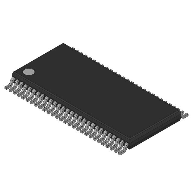
Harris Corporation CD74LPT16501AMT


- Part Number:
CD74LPT16501AMT
- Manufacturer:
- Category:
- RoHs:
 Non-RoHS Compliant
 - Datasheet:
- Description:
IC TXRX NON-INVERT 3.6V 56TSSOP
- In stock 3,010

CD74LPT16501AMT Fast CMOS 18‑Bit Registered Transceiver – Full Datasheet Summary
1. Basic Information
- Manufacturer: Harris Corporation
- Release Date: December 1996
- Device Type: Fast CMOS 18‑bit registered bus transceiver
- Technology: 0.6‑μm advanced CMOS, compatible with LCX™ families
- Part Number: CD74LPT16501AMT
- Application: 3.3V/5V mixed‑signal bus translation, registered bidirectional data transfer
2. Key Features
- 5V‑tolerant mixed‑signal operation: inputs accept 3V/5V; outputs connect to 3V or 5V buses
- Low‑power CMOS operation
- Balanced 24 mA sink/source output drive
- Pin‑compatible with industry standard double‑density pinouts
- Low ground‑bounce outputs
- Hysteresis on all inputs
- Multiple center and distributed VCC/GND pins to minimize switching noise
- Flow‑through pinout for easy PCB layout
- Supports transparent, latched, and clocked data modes via D‑type latches and flip‑flops
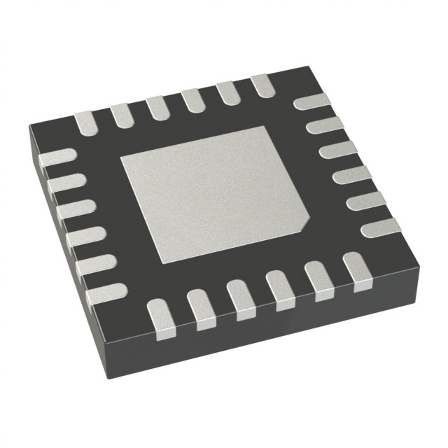
3. Ordering & Packaging (CD74LPT16501AMT)
| Parameter | Value |
|---|---|
| Temperature Range | −40°C to +85°C |
| Package | 56‑lead TSSOP |
| Package Code | M56.240‑P |
| Tape‑and‑Reel Suffix | Add “96” (CD74LPT16501AMT96) |
4. Functional Description
The device is an 18‑bit bidirectional registered transceiver with independent control for A→B and B→A directions.
- Control signals:
- Modes:
- B→A operation mirrors A→B using OEBA, LEBA, CLKBA
5. Truth Table (A→B Direction)
| OEAB | LEAB | CLKAB | Ax | Bx | Notes |
|---|---|---|---|---|---|
| L | X | X | X | Z | Output disabled |
| H | H | X | L | L | Transparent |
| H | H | X | H | H | Transparent |
| H | L | ↑ | L | L | Clock‑edge triggered |
| H | L | ↑ | H | H | Clock‑edge triggered |
| H | L | L | X | Hold | Latched |
| H | L | H | X | Hold | Latched |
| Notes: H=High, L=Low, X=Don’t care, ↑=Low‑to‑High transition, Z=High impedance |
6. Absolute Maximum Ratings
| Parameter | Rating |
|---|---|
| DC Input Voltage | −0.5V to +7.0V |
| DC Output Current | 120 mA |
| Storage Temperature | −65°C to +150°C |
| Max Lead Soldering Temp (10s) | 300°C (lead tips only) |
| Max Junction Temp | 150°C |
7. Operating Conditions
- Supply Voltage (VCC): 2.7V to 3.6V
- Operating Temperature: −40°C to +85°C
- Input Voltage Range: −0.5V to +5.5V
8. DC Electrical Specifications (TA = −40 to 85°C, VCC = 2.7–3.6V)
| Parameter | Symbol | Min | Max | Unit |
|---|---|---|---|---|
| Input HIGH Voltage (input pins) | VIH | 2.2 | 5.5 | V |
| Input HIGH Voltage (I/O pins) | VIH | 2.0 | 5.5 | V |
| Input LOW Voltage (all) | VIL | −0.5 | 0.8 | V |
| Input Leakage Current | II | — | ±1 | μA |
| Output HIGH Voltage (IOH = −24 mA) | VOH | 2.0 | — | V |
| Output LOW Voltage (IOL = 24 mA) | VOL | — | 0.5 | V |
| Clamp Diode Voltage | VIK | — | −1.2 | V |
| Power‑Down Leakage (IOFF) | — | — | ±100 | μA |
| Input Hysteresis | VH | 150 | — | mV |
9. Capacitance (TA = 25°C, f = 1 MHz)
| Parameter | Symbol | Typ | Max | Unit |
|---|---|---|---|---|
| Input Capacitance | CIN | 4.5 | 6 | pF |
| Output Capacitance | COUT | 5.5 | 8 | pF |
10. Power Supply Characteristics
| Parameter | Condition | Typ | Max | Unit |
|---|---|---|---|---|
| Quiescent Current (ICC) | VIN = GND | 0.1 | 10 | μA |
| Quiescent TTL Input | VIN = VCC−0.6V | 2.0 | 30 | μA |
| Dynamic Supply Current | 1‑bit toggling | — | 50–75 | μA |
| Total ICC (18‑bit, 10 MHz) | — | 0.6–2.1 | 2.3–4.7 | mA |
11. Switching Specifications (CL = 50 pF, RL = 500Ω, VCC = 3.3V±0.3V)
| Parameter | CD74LPT16501 | CD74LPT16501A | Unit |
|---|---|---|---|
| Max Clock Frequency | — | 150 | MHz |
| Propagation Delay (Ax↔Bx) | 1.5–6.5 | 1.5–5.1 | ns |
| Propagation Delay (LE→Ax/Bx) | 1.5–7.5 | 1.5–5.6 | ns |
| Propagation Delay (CLK→Ax/Bx) | 1.5–8.0 | 1.5–5.6 | ns |
| Output Enable Time | 1.5–8.0 | 1.5–6.0 | ns |
| Output Disable Time | 1.5–7.5 | 1.5–5.6 | ns |
| Setup Time (Data→CLK) | 4.0 | 3.0 | ns |
| Hold Time (Data→CLK) | 0 | 0 | ns |
| Pulse Width (CLK/LE) | 3.0 | 3.0 | ns |
| Output Skew | 0.5 | 0.5 | ns |
12. Thermal Information
| Package | θJA (Typical) |
|---|---|
| TSSOP (AMT) | 85°C/W |
| SSOP | 70°C/W |
13. Pinout Overview (56‑Ld TSSOP/SSOP, Top View)
- Control: OEAB, LEAB, CLKAB, OEBA, LEBA, CLKBA
- Data Ports: A0–A17, B0–B17
- Power: Multiple VCC and GND pins distributed for noise reduction
14. Cautions
- ESD‑sensitive device; follow proper IC handling procedures
- Absolute maximum ratings are stress ratings only; not for continuous operation
- Do not short multiple outputs simultaneously; short‑circuit test limited to <1 second
Purchase
No need to register to order from JMBom Electronics, but signing in lets you track your order like a pro. Give it a try for a smoother shopping ride.
Means
Easy peasy! Pay your way with PayPal, Credit Card, or wire transfer in USD. We've got you covered.
RFQ(Request for Quotations)
Get the freshest prices and stock updates by asking for a quote! Our sales team will shoot you an email within a day. It's that simple.
IMPORTANT NOTICE
1. Look out for your order details in your inbox! (If it's missing, check the spam folder just in case.)
2. Our sales manager will double-check the order and keep you posted on any price or stock changes. No worries, we've got you covered.

Shipping Rate
We ship orders once a day around 5 p.m., except Sunday. Once shipped, the estimated delivery time depends on the courier company you choose, usually 5-7 working days.

Shipping Methods
We provide DHL, FedEx, UPS, EMS, SF Express, and Registered Air Mail international shipping.


Payment
You can pay the orders on the website directly or pay by wire transfer offline. We support: Paypal、VISA、Credit Card.