
Infineon Technologies CY7C341B-25JC


- Part Number:
CY7C341B-25JC
- Manufacturer:
- Category:
- RoHs:
 Non-RoHS Compliant
 - Datasheet:
 CY7C341B-25JC_Datesheet
 - Description:
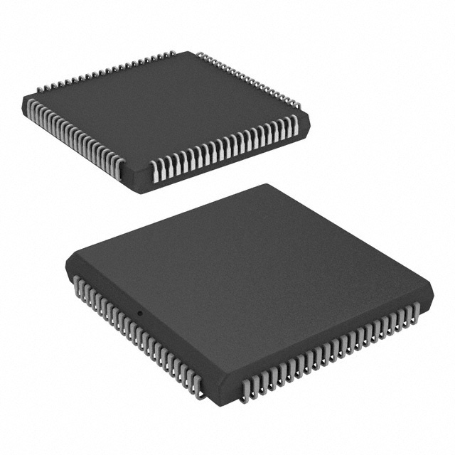
IC PLD 192MC 25NS 84PLCC
- In stock 0

CY7C341B-25JC Accessory Model Information
(Comprehensive Data Sheet Extract & Application Notes)
1. Device Identity
| Item | Details |
|---|---|
| Ordering Code | CY7C341B-25JC (Commercial temp) / CY7C341B-25JI (Industrial temp) |
| Marketing Name | 192-Macrocell MAX® EPLD |
| Family | Cypress MAX® EPLD (Erasable-Programmable Logic Device) |
| Speed Grade | –25 (25 ns tPD1 combinatorial, 62.5 MHz fMAX) |
| Package | 84-lead Plastic Leaded Chip Carrier (PLCC-84), J83 outline |
| JEDEC | MS-018 registered, 1.15 in × 1.15 in body, 0.050 in lead pitch |
| RoHS Status | Non-RoHS (windowed for UV erasure) |
2. Pin-1 Reference & Pin-Use Summary
| Pin-1 Location | Corner index/dot next to pin 1 (top view) |
|---|---|
| Dedicated Inputs | 8 (incl. pin-3 global CLK) |
| Bi-dir I/O | 64 |
| Power | 8 VCC (pins 18-19-39-40-60-61-81-82) |
| Ground | 8 GND (pins 20-21-41-42-62-63-83-84) |
| NC | 0 – every pin has function |
3. Absolute Maximum Ratings (Stresses only)
| Parameter | Value |
|---|---|
| VCC w.r.t. GND | –0.5 V to +7.0 V |
| DC I/O voltage | –0.5 V to VCC + 0.5 V |
| DC output current per pin | ±50 mA |
| Storage temperature | –65 °C to +135 °C |
| TJ (junction) under bias | 150 °C |
4. Recommended Operating Conditions
| Grade | Ambient Temp | VCC Tolerance |
|---|---|---|
| Commercial (C) | 0 °C to +70 °C | 5 V ± 5 % |
| Industrial (I) | –40 °C to +85 °C | 5 V ± 10 % |
5. DC Electrical Characteristics (over operating range)
| Symbol | Parameter | Min | Max | Unit |
|---|---|---|---|---|
| VIH | Input HIGH | 2.0 | VCC+0.3 | V |
| VIL | Input LOW | –0.3 | 0.8 | V |
| VOH | Output HIGH (IOH = –4 mA) | 2.4 | – | V |
| VOL | Output LOW (IOL = 8 mA) | – | 0.45 | V |
| IIX | Input leakage | –10 | +10 | µA |
| IOZ | Tri-state leakage | –40 | +40 | µA |
6. Switching Characteristics (CY7C341B-25JC)
| Symbol | Description | Min | Max | Unit |
|---|---|---|---|---|
| tPD1 | Dedicated input → comb. output | – | 25 | ns |
| tPD2 | I/O input → comb. output | – | 40 | ns |
| tSU | Global CLK set-up time | 15 | – | ns |
| tCO1 | CLK → registered output | – | 14 | ns |
| fMAX | Max toggle frequency (pipeline) | 62.5 | – | MHz |
7. On-Chip Resources
| Block | Quantity | Details |
|---|---|---|
| Logic Array Blocks (LABs) | 12 | 16 macrocells each |
| Macrocells | 192 | 64 I/O-linked, 128 buried |
| Expander Product Terms | 384 | 32 per LAB, shareable |
| Product-Term Expanders | 384 | Single-term, 32 per LAB |
| PIA (Programmable Interconnect) | 1 | Fixed 14 ns delay, zero skew |
8. Design-Security & Erase
- Security bit prohibits EPROM read-back; erased by 20-30 min UV @ 3.6 mW/cm², 253.7 nm.
- Window: Quartz lid – keep covered during normal operation.
9. Accessory & Support Components
| Function | Cypress Part / Recommendation |
|---|---|
| Device Socket | 84-contact PLCC socket, 0.050 in pitch (e.g. Mill-Max 054-1-084) |
| UV Eraser | Cypress CE-220 or equivalent (3.6 mW/cm², 253.7 nm) |
| Software | CY3700/MAX+ pDS 4.x, later migrated to Altera MAX+PLUS II |
| Programming Adapter | Cypress CY3700-DIP84 for gang programmer |
| Power Decoupling | 0.22 µF mono-ceramic per VCC pin, placed < 0.5 in from package |
10. Thermal & Reliability Data
| Parameter | Typ | Unit | Condition |
|---|---|---|---|
| θJA (still air) | 45 | °C/W | J83 PLCC-84 |
| θJC | 15 | °C/W | Package top to case |
| Moisture sensitivity | JEDEC Level 3 | – | 168 h @ 30 °C/60 % RH |
11. Ordering & Packaging Codes
| Code | Description | Temp | Package |
|---|---|---|---|
| CY7C341B-25JC | Commercial | 0 °C – +70 °C | PLCC-84 (J83) |
| CY7C341B-25JI | Industrial | –40 °C – +85 °C | PLCC-84 (J83) |
| CY7C341B-25HC/HI | Windowed LCC | C/I | HLCC-84 (H84) |
| CY7C341B-25RC/RI | Windowed PGA | C/I | PGA-84 (R84) |
12. Handling & Design Tips
- Unused inputs: Tie to VCC or GND – do not float.
- Unused I/Os: Configure as output driving LOW to minimize noise.
- Clocking: Use dedicated pin-3 for global CLK to achieve tSU/tCO specs.
- Power sequencing: VCC rise time ≤ 10 ms; apply simultaneous power to all VCC pins.
- Board lock: PLCC extractor tool prevents lead damage during removal.
Purchase
No need to register to order from JMBom Electronics, but signing in lets you track your order like a pro. Give it a try for a smoother shopping ride.
Means
Easy peasy! Pay your way with PayPal, Credit Card, or wire transfer in USD. We've got you covered.
RFQ(Request for Quotations)
Get the freshest prices and stock updates by asking for a quote! Our sales team will shoot you an email within a day. It's that simple.
IMPORTANT NOTICE
1. Look out for your order details in your inbox! (If it's missing, check the spam folder just in case.)
2. Our sales manager will double-check the order and keep you posted on any price or stock changes. No worries, we've got you covered.

Shipping Rate
We ship orders once a day around 5 p.m., except Sunday. Once shipped, the estimated delivery time depends on the courier company you choose, usually 5-7 working days.

Shipping Methods
We provide DHL, FedEx, UPS, EMS, SF Express, and Registered Air Mail international shipping.


Payment
You can pay the orders on the website directly or pay by wire transfer offline. We support: Paypal、VISA、Credit Card.


Infineon Technologies
Infineon Technologies
Infineon Technologies
Infineon Technologies
Infineon Technologies
Infineon Technologies
Infineon Technologies
Infineon Technologies
Infineon Technologies
Infineon Technologies
Infineon Technologies
Infineon Technologies