

 All Products
EPC FBS-GAM02P-R-PSE



- Part Number:
FBS-GAM02P-R-PSE
- Manufacturer:
- Category:
- RoHs:
 Non-RoHS Compliant
 - Datasheet:
- Description:
GAN DUAL HI/LO SIDE DRIVER 18SMT
- In stock 41



FBS-GAM02P-R-PSE Datasheet Comprehensive Summary
1. Overview
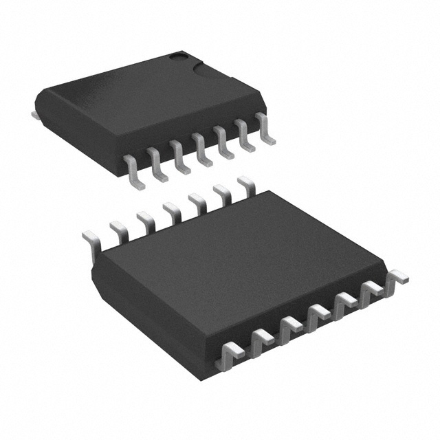
The FBS-GAM02P-R-PSE is a radiation-hardened, high-speed multifunction power gate driver module from EPC Space, designed based on the patented "GaN-Driving-GaN Technology". It integrates two independent high-speed gate drive circuits (composed entirely of eGaN® switching elements), a high-side driver bootstrap diode, input shoot-through prevention logic for half-bridge configurations, and +5 VDC gate drive bias power good monitoring circuitry. Packaged in an 18-pin SMT molded epoxy package with "pillar" I/O pads, this module is engineered to drive external EPC Space eGaN® HEMT power switches rated up to 100 VDC, with post-radiation effect guarantees and compliance with commercial 9A515.x device standards.
2. Key Features
2.1 Electrical & Functional Capabilities
- Voltage Operation: 50 VDC fully de-rated operation (100 VDC capable) with an internal 100 V-rated bootstrap diode.
- Gate Driver Configuration: Four flexible operating modes:
- Performance: High-speed switching capability (up to 3.0 MHz for low-side, 2.0 MHz for high-side), with dynamic gate/driver losses as low as 25 mW/MHz (per driver).
- Protection & Monitoring: Internal power good (PG) circuitry, under-voltage lockout (UVLO), over-voltage lockout (OVLO), and high/low-true shutdown inputs (*SD/SD).
2.2 Environmental & Mechanical Specifications
- Temperature Range: -55 °C to +110 °C (operating case temperature); -55 °C to +140 °C (storage junction temperature).
- Radiation Hardness:
- Package: Compact 18-pin SMT molded epoxy package with pillar I/O pads; dimensions: 1.00 × 0.75 × 0.125 inches.
- ESD Protection: Class 1A (Human Body Model).
3. Pin Configuration & Function
The module features 18 pins with dedicated functions for logic control, power supply, gate driving, and protection. Key pin details are summarized below:
| Pin # | Pin Name | I/O Type | Core Function | Key Notes |
|---|---|---|---|---|
| 1 | BIN | Input | Low-side switch logic input | Logic low (“0”) → BGATE low; logic high (“1”) → BGATE high |
| 2 | TIN | Input | High-side switch logic input | Logic low (“0”) → TGATE low; logic high (“1”) → TGATE high |
| 3 | LGND | -- | Logic ground | Must connect to system logic ground (low current) |
| 4 | VBIAS | Input | +5 VDC gate driver power supply | Recommend bypassing with 1.0 μF + 0.1 μF 25 V ceramic capacitors |
| 5 | PG | Output | Power good (open-drain) | Pull-up to VBIAS (4.7 kΩ resistor); low if VBIAS is outside UVLO/OVLO range |
| 6 | *SD | Input | Low-true shutdown | Pull to LGND to disable both gate drivers; leave open if unused |
| 7 | SD | Input | High-true shutdown | Pull to VBIAS to disable both gate drivers; leave open if unused |
| 8 | TOS | -- | Switching node sense | Internally connected to SN (Pin 12); return for bootstrap capacitor |
| 9 | N/C | -- | No internal connection | Recommended to tie to PGND (0 Ω jumper) for noise immunity |
| 10 | TBST | -- | High-side bootstrap supply | “+” connection for bootstrap capacitor; minimize trace length (high dV/dt) |
| 11 | TGATE | Output | High-side gate output | Connect to external high-side eGaN® HEMT gate; high dV/dt/dI/dt signal |
| 12 | SN | -- | High-side switching node | Connect to source sense (SS) of external high-side HEMT |
| 13 | BGATE | Output | Low-side gate output | Connect to external low-side eGaN® HEMT gate; high dV/dt/dI/dt signal |
| 14 | PGND | -- | Power ground | Connect to external low-side HEMT source; low-impedance path required |
| 15 | BCON | Input | Low-side shoot-through control | Tie to BSTP (Pin 16) for shoot-through protection; open if unused |
| 16 | BSTP | Output | Low-side shoot-through protection | Logical inverse of TIN; tie to BCON (Pin 15) for protection |
| 17 | TSTP | Output | High-side shoot-through protection | Logical inverse of BIN; tie to TCON (Pin 18) for protection |
| 18 | TCON | Input | High-side shoot-through control | Tie to TSTP (Pin 17) for shoot-through protection; open if unused |
4. Electrical Specifications
4.1 Absolute Maximum Ratings (TC = 25 °C)
| Parameter | Value | Unit |
|---|---|---|
| SN to PGND Voltage | 50 | V |
| BGATE/TGATE Output Capacitance | 10,000 | pF |
| VBIAS Voltage Range | -0.3 to 6.5 | V |
| BIN/TIN Input Voltage Range | -0.3 to 5.0 | V |
| Junction Operating Temperature (TJ) | -55 to +130 | °C |
| Case Operating Temperature (TC) | -55 to +110 | °C |
| ESD (HBM) | Class 1A | -- |
4.2 Typical Electrical Characteristics (TC = 25 °C, VBIAS = 5 VDC)
Gate Driver Output (BGATE/TGATE)
| Parameter | Symbol | Test Conditions | Min | Typ | Max | Unit |
|---|---|---|---|---|---|---|
| BGATE Low-Level Voltage | VOL | IB GATE = 50 μA | -- | 0.05 | 0.10 | VDC |
| BGATE High-Level Voltage | VOH | IB GATE = -50 μA | 4.90 | 4.95 | -- | VDC |
| BGATE Pull-Down ON-Resistance | RDS(on) | IB GATE = 0.25 A | -- | 2.5 | 3.5 | Ω |
| TGATE High-Level Voltage | VOH | IT GATE = -50 μA, SN = 0 V | 4.45 | 4.55 | -- | VDC |
| TGATE Pull-Up ON-Resistance | RDS(on) | IT GATE = -0.25 A | -- | 2.5 | 3.5 | Ω |
Switching Performance
| Parameter | Symbol | Test Conditions | Typ | Max | Unit |
|---|---|---|---|---|---|
| BIN-to-BGATE Turn-On Delay | td(on) | COUT = 2200 pF | -- | 30 | ns |
| TIN-to-TGATE Turn-On Delay | td(on) | COUT = 2200 pF | -- | 65 | ns |
| BGATE Rise Time (tr) | tr | COUT = 2200 pF | 42 | 45 | ns |
| TGATE Fall Time (tf) | tf | COUT = 2200 pF | 38 | 45 | ns |
Power Good (PG) & UVLO/OVLO
| Parameter | Symbol | Test Conditions | Min | Typ | Max | Unit |
|---|---|---|---|---|---|---|
| VBIAS UVLO Rising Threshold | UVLO+ | -- | -- | -- | 4.45 | V |
| VBIAS UVLO Falling Threshold | UVLO- | -- | 2.95 | -- | -- | V |
| VBIAS OVLO Rising Threshold | OVLO+ | -- | -- | -- | 6.70 | V |
| PG Low-Level Voltage | VOL | Pull-up = 4.7 kΩ | -- | -- | 0.2 | V |
5. Recommended External Components
5.1 eGaN® HEMT Power Transistors
The module is optimized to drive EPC Space eGaN® HEMTs. Recommended models for different voltage/current requirements are:
| VDD (VDC) | IO (ADC) | EPC Space P/N | RDS(on) (mΩ) | Package |
|---|---|---|---|---|
| 40 | 8 | FBG04N08AX | 24 | FSMD-A |
| 40 | 30 | FBG04N30BX | 6 | FSMD-B |
| 100 | 5 | FBG10N05AX | 38 | FSMD-A |
| 100 | 30 | FBG10N30BX | 9 | FSMD-B |
5.2 Bypass & Bootstrap Components
- VBIAS Bypass: 1.0 μF + 0.1 μF 25 V ceramic capacitors (between VBIAS (Pin 4) and PGND (Pin 14)).
- Bootstrap Capacitor: 1 μF external capacitor (between TBST (Pin 10) and TOS (Pin 8)) + internal 47 nF capacitor.
6. Typical Applications
The FBS-GAM02P-R-PSE is suitable for high-reliability, high-speed power conversion and motor control systems, including:
- High-Speed DC-DC Conversion: POL (Point of Load) converters, high-current DC-DC converters.
- Motor Drives: Single/multi-phase motor phase drivers (e.g., aerospace actuation systems).
- Power Switches: High-voltage power switches/actuators in avionics.
- Space Electronics: Commercial satellite EPS (Electrical Power Systems) and avionics power modules.
6.1 Key Application Circuits
- Single High-Side Configuration: Drives a high-side eGaN® HEMT (Qext) with PWM input to TIN (Pin 2); SN (Pin 12) connects to Qext source.
- Half-Bridge Configuration: Integrates low-side (Qext1) and high-side (Qext2) HEMTs with shoot-through protection (BCON-BSTP and TCON-TSTP tied); outputs regulated voltage (VOUT = VDD × (ton/T)).
7. PCB Design Guidelines
7.1 Solder Pad Configuration
- Follow the recommended PCB solder pad dimensions (see Figure 19 in the original datasheet) for optimal thermal/electrical performance.
- Use Sn63/Pb37 no-clean solder paste; maximum peak reflow temperature: 230 °C (dwell time < 4.5 minutes).
7.2 Layout Best Practices
- High-Speed Signals: Minimize trace lengths for TGATE (Pin 11), BGATE (Pin 13), and SN (Pin 12) to reduce EMI and voltage ringing.
- Grounding: Separate LGND (logic ground) and PGND (power ground); connect PGND to a low-impedance power ground plane.
- Bypassing: Place VBIAS bypass capacitors as close to Pin 4 (VBIAS) and Pin 14 (PGND) as possible.
8. Ordering Information & Part Number Decoding
The part number FBS-GAM02P-R-PSE follows EPC Space’s naming convention:
- FBS: Product family (GaN adaptor module).
- GAM02P: Model identifier (multifunction gate driver, molded plastic package).
- R: Radiation-hardened grade.
- PSE: Power switch external driver (application type).
- No additional suffixes are required for tape-and-reel packaging; standard shipping is in tape-and-reel format.
9. Radiation & Reliability
- Total Ionizing Dose (TID): Guaranteed to survive 100 kRad (Si) under high dose rate, with parametric stability pre/post-radiation.
- Single Event Effects (SEE): Immune to heavy ions (Au, LET = 83.7 MeV·cm²/mg) to prevent latch-up or burnout.
- Quality Assurance: 100% wafer-by-wafer radiation-hardness validation for eGaN® elements; compliant with Mil-Std-750 Method 1019.
Purchase
No need to register to order from JMBom Electronics, but signing in lets you track your order like a pro. Give it a try for a smoother shopping ride.
Means
Easy peasy! Pay your way with PayPal, Credit Card, or wire transfer in USD. We've got you covered.
RFQ(Request for Quotations)
Get the freshest prices and stock updates by asking for a quote! Our sales team will shoot you an email within a day. It's that simple.
IMPORTANT NOTICE
1. Look out for your order details in your inbox! (If it's missing, check the spam folder just in case.)
2. Our sales manager will double-check the order and keep you posted on any price or stock changes. No worries, we've got you covered.

Shipping Rate
We ship orders once a day around 5 p.m., except Sunday. Once shipped, the estimated delivery time depends on the courier company you choose, usually 5-7 working days.

Shipping Methods
We provide DHL, FedEx, UPS, EMS, SF Express, and Registered Air Mail international shipping.


Payment
You can pay the orders on the website directly or pay by wire transfer offline. We support: Paypal、VISA、Credit Card.