Sanyo LC749402BG-TLM-H


- Part Number:
LC749402BG-TLM-H
- Manufacturer:
- Category:
- RoHs:
 RoHS Compliant
 - Datasheet:
- Description:
LCD PICTURE QUALITY IMPROVEMENT
- In stock 2,000

LC749402BG-TLM-H LCD Picture Quality Improvement IC Product Information Summary
1. General Description
The LC749402BG-TLM-H is a high-performance LCD picture quality improvement IC developed by ON Semiconductor. It processes output signals for LCD panels to deliver enhanced display quality, supporting up to WVGA/SVGA panels (max 896 horizontal dots, 768 vertical lines) with an operating frequency of 40 MHz or less. The device integrates comprehensive image quality correction functions for YCbCr/YPbPr, RGB, and Y signals, along with a built-in panel driver timing controller and backlight control PWM. It features digital input/output (24-bit YCbCr/RGB, 16-bit 4:2:2, 8-bit ITU-R BT.656) and communicates via I²C or 4-wire SIO interface. Housed in a 96-lead FBGA package (6.0×6.0 mm), it operates over a temperature range of -40 °C to +85 °C, making it ideal for LCD display equipment requiring precise image adjustment and low-power operation.
2. Core Features and Benefits
2.1 Image Quality Correction
- Y Signal Enhancement: Luminance adjustment, contour correction, Color Depth Expander (CDEX), dynamic-γ correction, and black/white stretch.
- Color Signal Optimization: Color exciter, flesh tone correction, hue adjustment, and color gain control for YCbCr/YPbPr signals.
- RGB Signal Tuning: Brightness, contrast, white balance, black balance, and γ correction for RGB inputs.
- Dithering Function: Reduces quantization noise for smoother gradient transitions.
2.2 Signal Input/Output Flexibility
- Digital Inputs: Supports 24-bit YCbCr/YPbPr (4:4:4), 16-bit YCbCr (4:2:2), 8-bit ITU-R BT.656, and 24-bit RGB signals.
- Digital Outputs: Provides 18-bit/24-bit RGB and 16-bit (4:2:2)/24-bit (4:4:4) YCbCr signals.
- OSD Mixing: Integrates OSD (On-Screen Display) mixing functionality for overlay graphics.
2.3 Panel Control & Protection
- Built-in TCON: Timing controller for panel driver synchronization (horizontal/vertical sync, data enable, strobe signals).
- Panel Protection: Generates protection timing signals to prevent panel damage.
- Backlight Control: PWM output for video-adaptive backlight dimming, reducing power consumption.
2.4 System Compatibility
- Dual Interface Support: I²C (slave mode) and 4-wire SIO for register configuration.
- Flexible Power Supplies: Core voltage (1.0–1.3 V) and I/O voltage (1.7–1.9 V or 2.6–3.6 V) to match system requirements.
- Low Power Consumption: Static supply current of 20 μA (typ) and dynamic current of 18 mA (10 MHz) to 57 mA (40 MHz).
3. Applications
- LCD display equipment (monitors, TVs, industrial displays)
- Portable LCD devices (tablets, portable media players)
- Automotive LCD displays (infotainment systems, instrument clusters)
- Industrial control panels and medical LCD monitors
4. Key Electrical Specifications
4.1 Absolute Maximum Ratings (Ta=25 °C, DVSS=0 V, AVSS_OSC=0 V)
| Parameter | Symbol | Ratings | Unit |
|---|---|---|---|
| I/O Supply Voltage | DVDD_IO | -0.3 to +3.96 | V |
| Core/Analog Oscillator Supply Voltage | DVDD_CORE, AVDD_OSC | -0.3 to +1.8 | V |
| Digital Input Voltage | VI | -0.3 to DVDD_IO + 0.3 | V |
| Digital Output Voltage | VO | -0.3 to DVDD_IO + 0.3 | V |
| Operating Temperature | Topr | -40 to +85 | °C |
| Storage Temperature | Tstg | -55 to +125 | °C |
4.2 Recommended Operating Conditions (Ta=-40 to +85 °C, DVSS=0 V, AVSS_OSC=0 V)
| Parameter | Symbol | Min | Typ | Max | Unit |
|---|---|---|---|---|---|
| I/O Supply Voltage | DVDD_IO | 1.7 | 1.8 | 1.9 | V |
| I/O Supply Voltage | DVDD_IO | 2.6 | 2.85 | 3.6 | V |
| Core/Analog Oscillator Supply Voltage | DVDD_CORE, AVDD_OSC | 1.0 | 1.2 | 1.3 | V |
| Input Voltage Range | VIN | 0 | - | DVDD_IO | V |
| Maximum Operating Frequency | fCLK | - | - | 40 | MHz |
4.3 DC Characteristics (Ta=-40 to +85 °C)
| Parameter | Symbol | Conditions | Min | Typ | Max | Unit |
|---|---|---|---|---|---|---|
| Input High-Level Voltage | VIH | CMOS inputs | 0.7DVDD_IO | - | - | V |
| Input Low-Level Voltage | VIL | CMOS inputs | - | - | 0.3DVDD_IO | V |
| Input High-Level Current | IIH | VI=DVDD_IO | - | - | 10 | μA |
| Input Low-Level Current | IIL | VI=DVSS | -10 | - | - | μA |
| Output High-Level Voltage | VOH | IOH=-4 mA (DVDD_IO=2.6–3.6 V) | DVDD_IO - 0.4 | - | - | V |
| Output Low-Level Voltage | VOL | CMOS outputs | - | - | 0.4 | V |
| Output Leakage Current | IOZ | High-impedance output | -10 | - | 10 | μA |
| Pull-Down Resistor | RDN | Ta=25 °C, DVDD_IO=2.85 V | - | 98 | - | kΩ |
| Static Supply Current | IDDST | Ta=25 °C, outputs open | - | 20 | - | μA |
| Dynamic Supply Current | IDDOP | Ta=25 °C, tck=10 MHz | - | 18 | - | mA |
| Dynamic Supply Current | IDDOP | Ta=25 °C, tck=40 MHz | - | 57 | - | mA |
4.4 Timing Characteristics
4.4.1 Input Timing
| Parameter | Symbol | Conditions | Min | Typ | Max | Unit |
|---|---|---|---|---|---|---|
| Clock Cycle | tCK | DCKI | 25 | - | - | ns |
| Clock Duty Cycle | - | DCKI | 50 | - | - | % |
| Input Data Setup Time | tSU | DVDD_IO=1.7–1.9 V | 3 | - | - | ns |
| Input Data Setup Time | tSU | DVDD_IO=2.6–3.6 V | 3 | - | - | ns |
| Input Data Hold Time | tHD | DVDD_IO=1.7–1.9 V | 2 | - | - | ns |
| Input Data Hold Time | tHD | DVDD_IO=2.6–3.6 V | 2 | - | - | ns |
4.4.2 Output Timing
| Parameter | Symbol | Conditions | Min | Typ | Max | Unit |
|---|---|---|---|---|---|---|
| Clock Cycle | tCK | DCKO | 25 | - | - | ns |
| Output Data Delay | tAC | DVDD_IO=2.6–3.6 V, 4mA drive | -3 | - | 3 | ns |
| Output Data Delay | tAC | DVDD_IO=2.6–3.6 V, 2mA drive | -3 | - | 6 | ns |
| Output Data Delay | tAC | DVDD_IO=1.7–1.9 V, 4mA drive | -5 | - | 4 | ns |
| Output Data Delay | tAC | DVDD_IO=1.7–1.9 V, 2mA drive | -6 | - | 9 | ns |
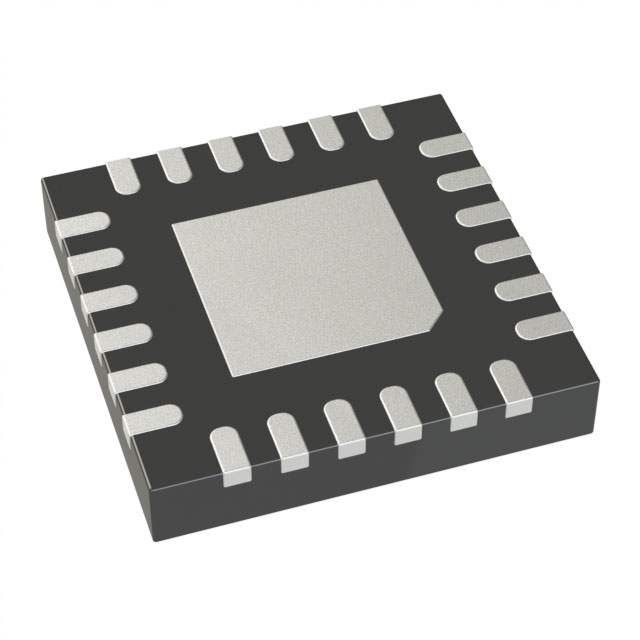
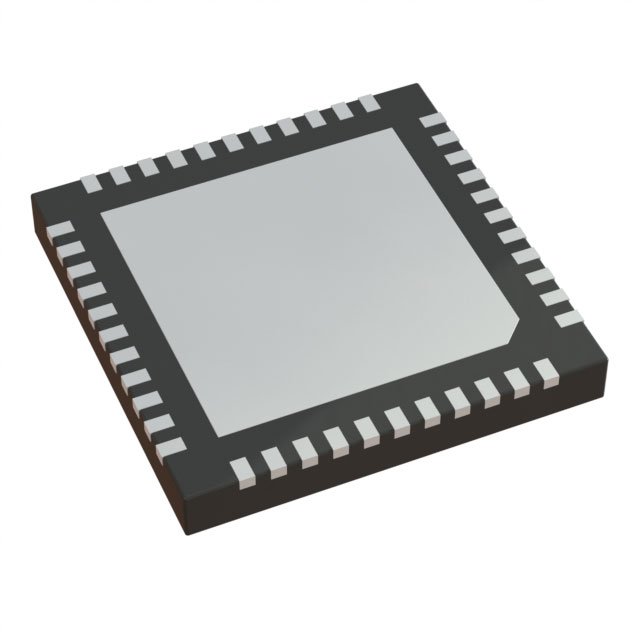
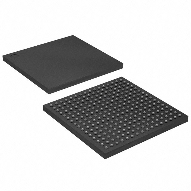
5. Pin Configuration and Description (96-Lead FBGA Package)
5.1 Key Pin Categories
| Pin Type | Key Pins | Function |
|---|---|---|
| Power Supplies | DVDD_IO, DVDD_CORE, AVDD_OSC | I/O supply (1.8V/3.3V), core supply (1.2V), analog oscillator supply |
| Ground Pins | DVSS, AVSS_OSC | Digital ground, analog oscillator ground |
| Signal Inputs | DCRIN[7:0], DYGIN[7:0], DCBIN[7:0] | RGB/Y/Cr, G/Y/656, B/Cb/C input signals |
| Signal Outputs | DROUT[7:0], DGOUT[7:0], DBOUT[7:0] | RGB/Y/Cr, G/Y, B/Cb/C output signals |
| Control Interface | SCK_SCL, SRXD_SDA, STXD, SIOSEL | I²C/SIO clock, data I/O, mode selection (I²C/SIO) |
| Timing Signals | DCKI, DCKO, DHSI, DVSO | Input/output video clock, horizontal/vertical sync |
| Panel Control | FLM, GRST, CPV, SP, OE, STRB | Gate/source driver control signals (start pulse, reset, enable) |
| Backlight Control | PWM | PWM output for backlight dimming |
| Reset & Power | XRST, PDWN | System reset (active low), power-down (active high) |
5.2 Critical Pin Notes
- RC_BIAS (B1): Connect to GND with a 20 kΩ resistor for bias configuration.
- TEST (D4): Normally connect to GND (built-in pull-down resistor).
- SIOSEL (G6): Select interface mode (LOW=I²C slave, HIGH=4-wire SIO).
- XTAL1 (K7): Clock input for panel protection and PWM generation; connect to GND if unused.
- Unused Input Pins: DCRIN[7:0], DYGIN[7:0], DCBIN[7:0] must be connected to GND when not in use.
6. Functional Operation
6.1 Image Processing Flow
- Signal Input: Accepts RGB, YCbCr/YPbPr, or ITU-R BT.656 digital signals.
- Quality Correction: Applies luminance, color, and RGB-specific adjustments (e.g., contour correction, white balance, γ tuning).
- Color Space Conversion: Converts between YCbCr and RGB formats as needed.
- OSD Mixing: Overlays OSD signals onto the main video stream.
- Output Driving: Delivers corrected digital signals to the LCD panel, synchronized with timing controller outputs.
6.2 Panel Control
- Timing Controller: Generates horizontal/vertical sync (DHSO/DVSO), data enable (DDEO), and driver control signals (FLM, GRST, SP) for panel synchronization.
- Backlight Control: PWM output adapts to video content for low-power operation.
- Panel Protection: Generates protection timing signals to prevent overvoltage/overcurrent damage to the panel.
6.3 Interface Operation
- I²C Mode: Slave address selectable via SCS_I2SEL pin; supports register read/write for configuration.
- 4-Wire SIO Mode: Selected via SIOSEL pin; uses SCK_SCL (clock) and SRXD_SDA/STXD (data) for communication.
7. Package and Mechanical Specifications (96-Lead FBGA)
| Parameter | Typ | Unit |
|---|---|---|
| Package Length | 6.0 | mm |
| Package Width | 6.0 | mm |
| Package Height | 1.05 (max) | mm |
| Lead Pitch | 0.75 | mm |
| Ball Diameter | 0.5 | mm |
| Topside Marking | LC749402BG | - |
8. Application Guidelines
8.1 Power Supply Recommendations
- Decouple DVDD_IO, DVDD_CORE, and AVDD_OSC with 0.1 μF ceramic capacitors placed close to the pins.
- Ensure separate analog/digital ground planes connected at a single point to minimize noise.
8.2 Unused Pin Handling
- All unused input pins (DCRIN, DYGIN, DCBIN, etc.) must be tied to GND to avoid floating.
- TEST pin: Connect to GND for normal operation.
- PDWN pin: Connect to GND if power-down mode is not used.
8.3 PCB Layout Tips
- Route high-speed signals (DCKI, DCKO, data lines) with matched lengths to reduce skew.
- Keep power supply traces wide to minimize voltage drop.
- Isolate analog (AVDD_OSC, AVSS_OSC) and digital components to reduce interference.
Purchase
No need to register to order from JMBom Electronics, but signing in lets you track your order like a pro. Give it a try for a smoother shopping ride.
Means
Easy peasy! Pay your way with PayPal, Credit Card, or wire transfer in USD. We've got you covered.
RFQ(Request for Quotations)
Get the freshest prices and stock updates by asking for a quote! Our sales team will shoot you an email within a day. It's that simple.
IMPORTANT NOTICE
1. Look out for your order details in your inbox! (If it's missing, check the spam folder just in case.)
2. Our sales manager will double-check the order and keep you posted on any price or stock changes. No worries, we've got you covered.

Shipping Rate
We ship orders once a day around 5 p.m., except Sunday. Once shipped, the estimated delivery time depends on the courier company you choose, usually 5-7 working days.

Shipping Methods
We provide DHL, FedEx, UPS, EMS, SF Express, and Registered Air Mail international shipping.


Payment
You can pay the orders on the website directly or pay by wire transfer offline. We support: Paypal、VISA、Credit Card.