
Analog Devices Inc. LTM8049EY#PBF


- Part Number:
LTM8049EY#PBF
- Manufacturer:
- Category:
- RoHs:
 Non-RoHS Compliant
 - Datasheet:
- Description:
Non-Isolated PoL Module DC DC Converter 2 Output 2.5 ~ 24V -2.5 ~ -24V 1A 2.6V - 20V Input
- In stock 0

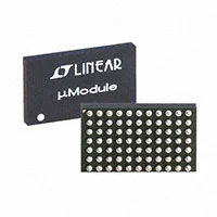
LTM8049EY#PBF Dual SEPIC/Inverting μModule DC/DC Converter
1. Basic Overview
- Device Type: Dual SEPIC or Inverting μModule DC/DC Converter
- Manufacturer: Analog Devices
- Part Number: LTM8049EY#PBF
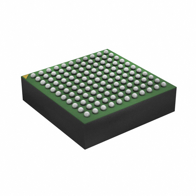
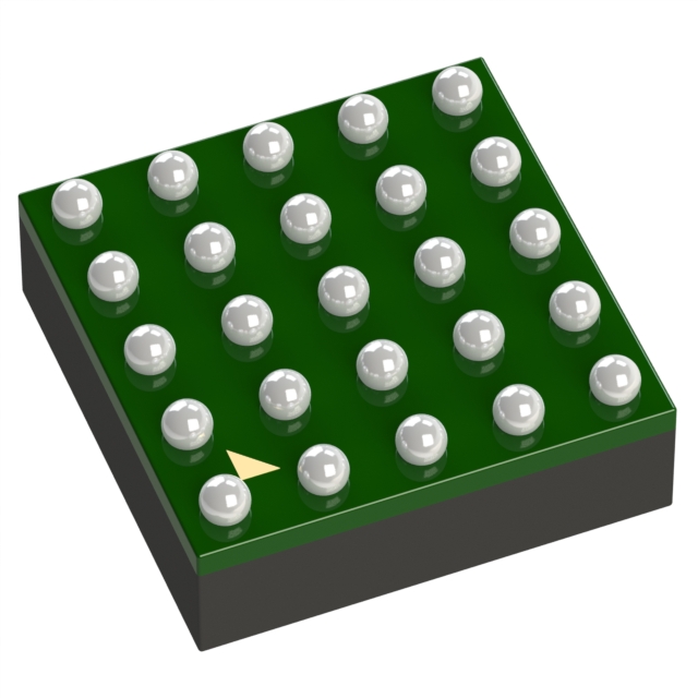
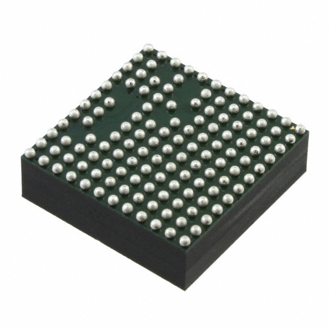
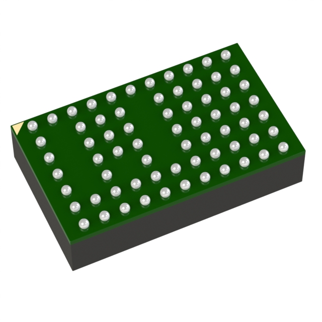
- Package: 77‑lead BGA, dimensions 15 mm × 9 mm × 2.42 mm
- Finish: SAC305, RoHS compliant (e4) with gold pad finish
- Temperature Grade: E‑grade; guaranteed 0°C to 125°C; performance over –40°C to 125°C assured by design
- MSL Rating: MSL 3
- Weight: 0.8 g
- Key Integration: Power devices, inductors, control circuitry, and passives integrated; minimal external components required
2. Key Features
- Dual independent switch‑mode power supplies
- Configurable as SEPIC or inverting topology
- Wide input voltage: 2.6 V to 20 V
- Output voltage:
- Output current: 1 A at 5 VOUT from 12 VIN; 0.25 A at 24 V/–24 V
- Switching frequency: 200 kHz to 2.5 MHz (resistor‑programmable or external sync)
- Power Good (PG) outputs for sequencing
- User‑configurable undervoltage lockout (UVLO)
- Soft‑start control via external capacitor
- Frequency synchronization input (SYNC) and clock output (CLKOUT)
- Thermal shutdown and overcurrent protection
- Low‑profile surface‑mount BGA for automated assembly
3. Absolute Maximum Ratings
- VINn, RUNn, PGn: 20 V
- SYNCn, FBXn: 5 V
- SSn: 2.5 V
- SHAREn: 2 V
- VOUTP (VOUTN = 0 V): 25 V
- VOUTN (VOUTP = 0 V): –25 V
- Maximum internal junction temperature: 125°C
- Storage temperature: –55°C to 125°C
- Maximum solder temperature: 260°C
4. Electrical Characteristics (TA = 25°C, unless noted)
表格
| Parameter | Condition | Min | Typ | Max | Unit |
|---|---|---|---|---|---|
| Minimum input operating voltage | — | 2.6 | — | — | V |
| Positive output voltage | IOut = 50 mA | — | 2.5 / 24 | — | V |
| Negative output voltage | IOut = 50 mA | — | –2.5 / –24 | — | V |
| Max continuous output current | VIN = 12 V, VOUT = 5 V/–5 V | 1 | — | — | A |
| VIN = 12 V, VOUT = 24 V/–24 V | 0.25 | — | — | A | |
| Quiescent current (RUN = 2 V, no load) | — | — | 10 | 2 | mA |
| RUN pin threshold (rising) | — | 1.21 | 1.31 | 1.4 | V |
| RUN pin threshold (falling) | — | — | 1.27 | — | V |
| Switching frequency range | RT programmed | 160 | — | 2900 | kHz |
| SYNC frequency range | — | 200 | — | 2500 | kHz |
| FBX regulation voltage (SEPIC) | — | 1.185 | 1.204 | 1.22 | V |
| FBX regulation voltage (inverting) | — | 20 | 2.7 | 120 | mV |
5. Thermal Specifications
- θJA: 16.2°C/W
- θJB: 3.8°C/W
- θJCtop: 8.8°C/W
- θJCbottom: 3.8°C/W
- θJCboard: 4.6°C/W
- Thermal shutdown: activates above 125°C; automatic recovery after cooling
6. Pin Functions Summary
- VIN1/VIN2: Input power; local bypass required
- VOUT1P/VOUT2P, VOUT1N/VOUT2N: Positive/negative outputs; grounding one sets topology
- RUN1/RUN2: Enable/disable; UVLO configuration
- RT1/RT2: Set switching frequency (resistor to GND)
- SS1/SS2: Soft‑start timing (capacitor to GND)
- SYNC1/SYNC2: External frequency synchronization
- FBX1/FBX2: Feedback for output voltage programming
- PG1/PG2: Open‑drain power‑good indicators
- CLKOUT1/CLKOUT2: Synchronization clock outputs
- SHARE1/SHARE2: Paralleling two outputs for higher current
- GND: System and thermal ground; must connect to VOUTP or VOUTN
7. Application Information
Topology Configuration
- SEPIC (positive output): Tie VOUTnN to GND
- Inverting (negative output): Tie VOUTnP to GND
Frequency Programming
- Formula: RT = (81.6 / fOSC) – 1 (fOSC in MHz, RT in kΩ)
- Recommended frequency: 200 kHz to 2.5 MHz
UVLO Configuration
- Single resistor: RUVLO1 = (VIN(TH) – 1.31 V) / 12.1 μA
- Two‑resistor for improved hysteresis stability
Capacitor Guidelines
- Input: 4.7 μF 25 V X5R/X7R ceramic (minimum)
- Output: X5R/X7R types; avoid Y5V/Z5U
- Bulk input capacitor recommended for hot‑plugging safety
PCB Layout
- Place CIN, COUT, RFB, RT close to device
- Large GND plane with thermal vias for heat dissipation
- Minimize loop areas to reduce EMI
8. Typical Applications
- Battery‑powered systems
- Local negative voltage regulators
- Low‑noise amplifier bias supplies
- Dual‑rail ±VOUT systems (e.g., ±5 V, ±12 V)
- Parallel outputs for higher output current
9. Ordering Information
- Part Number: LTM8049EY#PBF
- Package: 15 mm × 9 mm × 2.42 mm 77‑lead BGA
- Pad finish: SAC305 (RoHS)
- Temperature range: 0°C to 125°C (E‑grade)
- Not recommended for second‑side reflow; moisture‑sensitive device
Purchase
No need to register to order from JMBom Electronics, but signing in lets you track your order like a pro. Give it a try for a smoother shopping ride.
Means
Easy peasy! Pay your way with PayPal, Credit Card, or wire transfer in USD. We've got you covered.
RFQ(Request for Quotations)
Get the freshest prices and stock updates by asking for a quote! Our sales team will shoot you an email within a day. It's that simple.
IMPORTANT NOTICE
1. Look out for your order details in your inbox! (If it's missing, check the spam folder just in case.)
2. Our sales manager will double-check the order and keep you posted on any price or stock changes. No worries, we've got you covered.

Shipping Rate
We ship orders once a day around 5 p.m., except Sunday. Once shipped, the estimated delivery time depends on the courier company you choose, usually 5-7 working days.

Shipping Methods
We provide DHL, FedEx, UPS, EMS, SF Express, and Registered Air Mail international shipping.


Payment
You can pay the orders on the website directly or pay by wire transfer offline. We support: Paypal、VISA、Credit Card.


Analog Devices Inc.
Analog Devices Inc.

Analog Devices Inc.
Analog Devices Inc.
Analog Devices Inc.
Analog Devices Inc.

Analog Devices Inc.
Analog Devices Inc.
Analog Devices Inc.
Analog Devices Inc.
Analog Devices Inc.
Analog Devices Inc.