
Analog Devices Inc. ADL5561ACPZ-R7


- Part Number:
ADL5561ACPZ-R7
- Manufacturer:
- Category:
- RoHs:
 RoHS Compliant
 - Datasheet:
 ADL5561ACPZ-R7_Datesheet
 - Description:
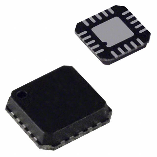
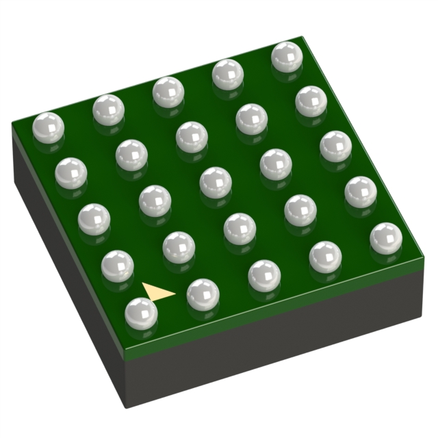
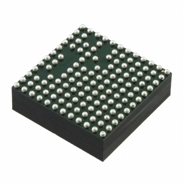
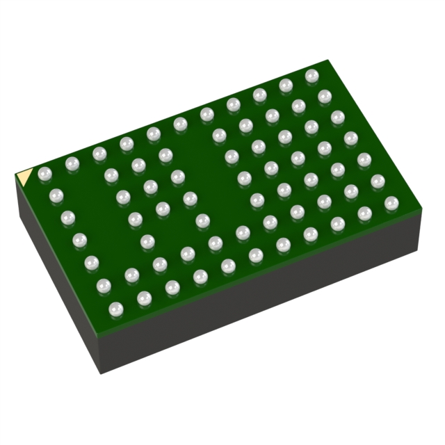
ADC Driver IC Driver 16-LFCSP-VQ (3x3)
- In stock 0

Product Specifications for ADL5562ACPZ-R7
Product Overview
The ADL5562ACPZ-R7 is a high-performance, differential amplifier optimized for RF and IF applications. It features low noise, low distortion, and high slew rate, making it suitable for driving high-speed ADCs and other broadband applications.
Key Features
- 3.3 GHz Ultralow Distortion RF/IF Differential Amplifier
- Pin-Strappable Gain Adjust: 6 dB, 12 dB, 15.5 dB
- Differential or Single-Ended Input to Differential Output
- Low Noise Input Stage: 2.1 nV/√Hz RTI at AV = 12 dB
- Low Broadband Distortion:10 MHz: −91 dBc HD2, −98 dBc HD370 MHz: −102 dBc HD2, −90 dBc HD3140 MHz: −104 dBc HD2, −87 dBc HD3250 MHz: −80 dBc HD2, −94 dBc HD3
- IMD3s of −94 dBc at 250 MHz Center
- Slew Rate: 9.8 V/ns
- Fast Settling of 2 ns and Overdrive Recovery of 3 ns
- Single-Supply Operation: 3 V to 3.6 V
- Power-Down Control
- Fabricated Using High-Speed XFCB3 SiGe Process
Applications
- Differential ADC Drivers
- Single-Ended to Differential Conversion
- RF/IF Gain Blocks
- SAW Filter Interfacing
General Description
The ADL5562 is a high-performance differential amplifier optimized for RF and IF applications. It offers low noise and excellent distortion performance over a wide frequency range, making it an ideal driver for high-speed 8-bit to 16-bit ADCs. The ADL5562 provides three gain levels through a pin-strappable configuration and can be configured for single-ended input. The quiescent current is typically 80 mA, and when disabled, it consumes less than 3 mA, offering excellent input-to-output isolation.
Ordering Information
- Model: ADL5562ACPZ-R7
- Temperature Range: -40°C to +85°C
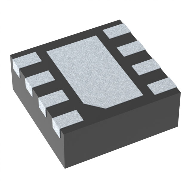
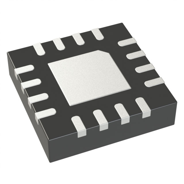
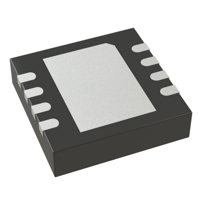
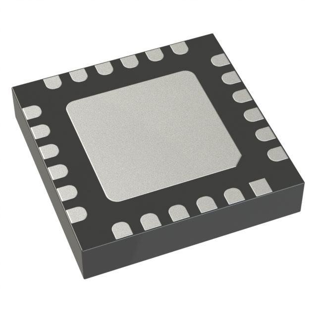
- Package: 16-Lead Lead Frame Chip Scale Package [LFCSP], 7” Tape and Reel
- Package Option: CP-16-22
- Ordering Quantity: 1,500 units
Specifications
- Supply Voltage (VCC): 3 V to 3.6 V
- ENBL Threshold:Device disabled, ENBL low: 0.5 VDevice enabled, ENBL high: 1.5 V
- ENBL Input Bias Current:ENBL high: -27 µAENBL low: -300 µA
- Quiescent Current:ENBL high: 75.5 mA to 84.5 mAENBL low: 3.5 mA
Dynamic Performance
- −3 dB Bandwidth:AV = 6 dB: 3300 MHzAV = 12 dB: 3900 MHzAV = 15.5 dB: 1900 MHz
- Bandwidth for 0.1 dB Flatness:AV = 6 dB: 220 MHzAV = 12 dB: 270 MHzAV = 15.5 dB: 270 MHz
- Gain Accuracy:AV = 6 dB: ±0.17 dBAV = 12 dB: ±0.05 dBAV = 15.5 dB: ±0.06 dB
- Gain Supply Sensitivity: -0.005 dB/V
- Gain Temperature Sensitivity: 0.32 mdB/°C
- Slew Rate:Rise, AV = 15.5 dB: 9.8 V/nsFall, AV = 15.5 dB: 10.1 V/ns
- Settling Time: 2 ns
- Overdrive Recovery Time: 3 ns
- Reverse Isolation (S12): 60 dB
Input/Output Characteristics
- Output Common Mode: VCC/2 V
- Voltage Adjustment Range: 1.4 to 1.8 V
- Maximum Output Voltage Swing: 4.9 V p-p (1 dB compressed)
- Output Common-Mode Offset: 60 mV
- Output Common-Mode Drift: 285 µV/°C
- Output Differential Offset Voltage: 1 mV
- CMRR: 65 dB
- Output Differential Offset Drift: 15 µV/°C
- Input Bias Current: 3 µA
- Input Resistance (Differential):AV = 6 dB: 400 ΩAV = 12 dB: 200 ΩAV = 15.5 dB: 133 Ω
- Input Resistance (Single-Ended):AV = 5.6 dB: 307 ΩAV = 11.1 dB: 179 ΩAV = 14.1 dB: 132 Ω
- Input Capacitance (Single-Ended): 0.3 pF
- Output Resistance (Differential): 12 Ω
Noise/Harmonic Performance
- Noise Spectral Density (RTI):AV = 6 dB: 3 nV/√HzAV = 12 dB: 2.1 nV/√HzAV = 15.5 dB: 1.6 nV/√Hz
- 1 dB Compression Point (RTO):AV = 6 dB: 13.5 dBmAV = 12 dB: 13.4 dBmAV = 15.5 dB: 13 dBm
Absolute Maximum Ratings
- Supply Voltage (VCC): 3.6 V
- VIP1, VIP2, VIN1, VIN2: VCC + 0.5 V
- Internal Power Dissipation: 310 mW
- θJA: 98.3°C/W
- Maximum Junction Temperature: 125°C
- Operating Temperature Range: -40°C to +85°C
- Storage Temperature Range: -65°C to +150°C
Pin Configuration and Function Descriptions
- VIP2: Balanced Differential Input. Biased to VCOM, typically ac-coupled. Input for AV = 12 dB gain, strapped to VIP1 for AV = 15.5 dB.
- VIP1: Balanced Differential Input. Biased to VCOM, typically ac-coupled. Input for AV = 6 dB gain, strapped to VIP2 for AV = 15.5 dB.
- VIN1: Balanced Differential Input. Biased to VCOM, typically ac-coupled. Input for AV = 6 dB gain, strapped to VIN2 for AV = 15.5 dB.
- VIN2: Balanced Differential Input. Biased to VCOM, typically ac-coupled. Input for AV = 12 dB gain, strapped to VIN1 for AV = 15.5 dB.
- VCC: Positive Supply.
- VCOM: Common-Mode Voltage. A voltage applied to this pin sets the common-mode voltage of the input and output. Typically decoupled to ground with a 0.1 µF capacitor.
- VON: Balanced Differential Output. Biased to VCOM, typically ac-coupled.
- VOP: Balanced Differential Output. Biased to VCOM, typically ac-coupled.
- ENBL: Enable. Apply positive voltage (1.0 V < ENBL < VCC) to activate device.
- GND: Ground. Connect to low impedance ground.
- EPAD: Exposed Pad. Connect to a low impedance thermal and electrical ground plane.
Typical Performance Characteristics
- Gain vs. Frequency Response: Figures 3 and 4 show the gain response for different gains and loads over temperature.
- Noise Figure: Figure 5 shows the noise figure vs. frequency for different gains.
- Output P1dB: Figures 6 and 7 show the output P1dB vs. frequency for different gains and loads over temperature.
Purchase
No need to register to order from JMBom Electronics, but signing in lets you track your order like a pro. Give it a try for a smoother shopping ride.
Means
Easy peasy! Pay your way with PayPal, Credit Card, or wire transfer in USD. We've got you covered.
RFQ(Request for Quotations)
Get the freshest prices and stock updates by asking for a quote! Our sales team will shoot you an email within a day. It's that simple.
IMPORTANT NOTICE
1. Look out for your order details in your inbox! (If it's missing, check the spam folder just in case.)
2. Our sales manager will double-check the order and keep you posted on any price or stock changes. No worries, we've got you covered.

Shipping Rate
We ship orders once a day around 5 p.m., except Sunday. Once shipped, the estimated delivery time depends on the courier company you choose, usually 5-7 working days.

Shipping Methods
We provide DHL, FedEx, UPS, EMS, SF Express, and Registered Air Mail international shipping.


Payment
You can pay the orders on the website directly or pay by wire transfer offline. We support: Paypal、VISA、Credit Card.


Analog Devices Inc.
Analog Devices Inc.
Analog Devices Inc.
Analog Devices Inc.
Analog Devices Inc.
Analog Devices Inc.

Analog Devices Inc.
Analog Devices Inc.
Analog Devices Inc.
Analog Devices Inc.
Analog Devices Inc.
Analog Devices Inc.