
Micron Technology Inc. MT40A512M16LY-062E IT:E


- Part Number:
MT40A512M16LY-062E IT:E
- Manufacturer:
- Category:
- RoHs:
 Non-RoHS Compliant
 - Datasheet:
- Description:
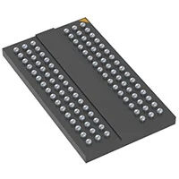
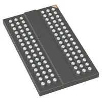
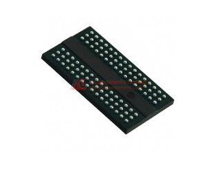
SDRAM - DDR4 Memory IC 8Gbit Parallel 1.6 GHz 96-FBGA (7.5x13.5)
- In stock 0

MT40A512M16LY‑062E IT:E Comprehensive Datasheet Summary
1. Basic Device Information
- Full Part Number: MT40A512M16LY‑062E IT:E
- Device Type: 8Gb Industrial‑grade DDR4 SDRAM
- Organization: 512M × 16‑bit (x16)
- Manufacturer: Micron Technology
- Document: 8Gb DDR4 SDRAM datasheet (Rev. L, Dec 2023)
- Status: Active
- Qualification: Industrial temperature grade (IT:E)
- Package: 96‑ball FBGA, 7.5 mm × 13.5 mm (Rev. E), Pb‑free, RoHS compliant
- Marking: LY, ‑062E, IT, E
2. Core Features
- Voltage: Core & I/O supply VDD/VDDQ = 1.2 V ± 60 mV; Boost VPP = 2.5 V −125/+250 mV
- Speed Grade: ‑062E; DDR4‑3200; tCK = 0.625 ns; CL = 22; tAA/tRCD/tRP = 13.75 ns
- Bank Architecture: 8 banks (2 bank groups × 4 banks each); 8n‑bit prefetch
- Internal Generation: On‑die adjustable VREFDQ generation
- I/O: 1.2 V pseudo open‑drain I/O
- Refresh: 8192‑cycle refresh; temperature‑compensated refresh (TCR)
- Reliability: Data Bus Inversion (DBI), Write CRC, CA Parity, Per‑DRAM Addressability (PDA)
- Power: Self refresh, Low‑Power Auto Self Refresh (LPASR), Self Refresh Abort
- Signal Integrity: Nominal/park/dynamic On‑Die Termination (ODT), ZQ calibration
- Compliance: JEDEC JESD79‑4 standard
3. Addressing & Page Size
| Parameter | Value |
|---|---|
| Bank Groups | 2 |
| Banks per Group | 4 |
| Row Address | A[15:0] (64K) |
| Column Address | A[9:0] (1K) |
| Page Size | 2 KB per bank |
4. Speed & Timing Parameters
| Speed Grade | Data Rate | CL‑RCD‑RP | tAA/tRCD/tRP |
|---|---|---|---|
| ‑062E | 3200 MT/s | 22‑22‑22 | 13.75 ns |
5. Operating Conditions
5.1 Temperature Ranges (Industrial, IT:E)
- Operating Case Temp (TC): −40 °C to +95 °C
- Storage Temp: −65 °C to +150 °C
- Refresh Intervals (8192 cycles):
5.2 Voltage Ratings
- VDD/VDDQ: 1.14 V to 1.26 V
- VPP: 2.375 V to 2.75 V
- Absolute Max Voltage: −0.5 V to 1.4 V for inputs/outputs
6. Pin Configuration (96‑Ball FBGA, Top View)
Key pins:
- Differential Clock: CK_t, CK_c
- Control: CKE, CS_n, ACT_n, RAS_n/A16, CAS_n/A15, WE_n/A14
- Address: A[17:0], BG0, BA[1:0], A10/AP, A12/BC_n
- Data: DQ[15:0], LDQS_t/LDQS_c, UDQS_t/UDQS_c
- Data Control: LDBI_n/LDM_n, UDBI_n/UDM_n
- Power: VDD, VDDQ, VPP, VSS, VSSQ, VREFCA
- Misc: RESET_n, ODT, PAR, ALERT_n, ZQ, TEN
7. Functional Description
7.1 Core Operation
- Architecture: 8n‑bit prefetch; double‑data‑rate transfer at I/O
- Commands: ACTIVATE, READ/WRITE, PRECHARGE, REFRESH, Self Refresh, MRS, ZQ Calibration
- Mode Registers: MR0–MR6 control timing, ODT, power, latency, CRC, DBI, parity, refresh modes
- MPR: Multipurpose Register for test, calibration, and status readback
7.2 Key Functions
- Write Leveling: For DIMM signal integrity
- Dynamic ODT: Adjustable termination during writes
- CAL: Command/Address Latency for power saving
- CRC: Write data cyclic redundancy check
- DBI: Data Bus Inversion for noise reduction
- CA Parity: Command/address parity protection
- PDA: Per‑DRAM Addressability for individual DRAM tuning
- PPR: Post Package Repair (soft sPPR supported)
8. Absolute Maximum Ratings
- Supply Voltage (VDD/VDDQ): −0.5 V to 1.4 V
- Input/Output Voltage: −0.5 V to 1.4 V
- DC Input Current: ± 150 mA
- Power Dissipation: 1.2 W
- Storage Temperature: −65 °C to +150 °C
9. Recommended Operating Conditions
- VDD/VDDQ: 1.14 V – 1.26 V
- VPP: 2.375 V – 2.75 V
- Ambient Temp (TA): −40 °C to +95 °C
- Clock Frequency: Up to 1600 MHz (3200 MT/s)
- Input Slew Rate: Compliant with JEDEC DDR4 specs
10. Electrical Characteristics
10.1 DC Parameters
- Input Leakage: ± 1 μA max
- Quiescent Current: Low active & standby currents
- ODT Impedance: Programmable 34/40/48/60/80/120/240 Ω
- Output Driver: 34/48 Ω programmable impedance
10.2 AC Parameters
- Propagation Delay: tAA = 13.75 ns
- CAS Latency: CL = 22
- Min Clock Pulse Width: Compliant with DDR4‑3200
- Data Setup/Hold: Compliant with JEDEC
11. Package & Mechanical Data
- Package: 96‑ball FBGA
- Dimensions: 7.5 mm × 13.5 mm × 1.20 mm
- Ball Pitch: Standard FBGA
- Solder Ball: SAC302 (Pb‑free)
- Moisture Sensitivity: MSL 3
- Thermal Resistance: RθJA ~ 45 °C/W (typical)
12. Ordering & Packaging
- Orderable Part: MT40A512M16LY‑062E IT:E
- Package Code: LY (96‑ball FBGA, 7.5 × 13.5 mm Rev. E)
- Speed: ‑062E (DDR4‑3200, CL22)
- Temperature: IT (Industrial, −40 °C to 95 °C)
- Revision: E
- Packing: Tape‑and‑reel, 2000 units per reel
13. Key Applications
- Industrial computing & automation
- Industrial servers & embedded systems
- Automotive infotainment (non‑safety)
- Networking & telecom infrastructure
- Ruggedized embedded designs
Purchase
No need to register to order from JMBom Electronics, but signing in lets you track your order like a pro. Give it a try for a smoother shopping ride.
Means
Easy peasy! Pay your way with PayPal, Credit Card, or wire transfer in USD. We've got you covered.
RFQ(Request for Quotations)
Get the freshest prices and stock updates by asking for a quote! Our sales team will shoot you an email within a day. It's that simple.
IMPORTANT NOTICE
1. Look out for your order details in your inbox! (If it's missing, check the spam folder just in case.)
2. Our sales manager will double-check the order and keep you posted on any price or stock changes. No worries, we've got you covered.

Shipping Rate
We ship orders once a day around 5 p.m., except Sunday. Once shipped, the estimated delivery time depends on the courier company you choose, usually 5-7 working days.

Shipping Methods
We provide DHL, FedEx, UPS, EMS, SF Express, and Registered Air Mail international shipping.


Payment
You can pay the orders on the website directly or pay by wire transfer offline. We support: Paypal、VISA、Credit Card.


Micron Technology Inc.

Micron Technology Inc.
Micron Technology Inc.

Micron Technology Inc.
Micron Technology Inc.
Micron Technology Inc.

Micron Technology Inc.

Micron Technology Inc.
Micron Technology Inc.
Micron Technology Inc.

Micron Technology Inc.
Micron Technology Inc.