
Macronix MX25V1635FZBI


- Part Number:
MX25V1635FZBI
- Manufacturer:
- Category:
- RoHs:
 Non-RoHS Compliant
 - Datasheet:
 MX25V1635FZBI_Datesheet
 - Description:
MEMORY
- In stock 0

MX25V1635FZBI – 16 Mbit (2 M × 8) 1.8 V Serial Multi-I/O NOR Flash
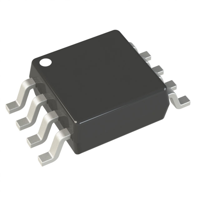
Macronix MXSMIO® Family – USON (4 mm × 3 mm) Package
1. Device Identity
TableCopy
| Item | Detail |
|---|---|
| Manufacturer | Macronix International Co., Ltd. |
| Base Part Number | MX25V1635F |
| Full Ordering Code | MX25V1635FZBI |
| Package | 8-land USON (4 mm × 3 mm, 0.8 mm pitch, 0.55 mm max height) |
| RohS / Halogen | Fully compliant, Pb-free, Halogen-free |
| Date-Codes | Rev. 1.4 (Sep 13 2016) onward |
2. Memory Array
- Density: 16 M-bit (2 M-byte)
- Organisation: 2,097,152 × 8 bit internally
- Uniform 4 k-byte sectors – 512 sectors total
- Uniform 32 k-byte blocks – 64 blocks total
- Uniform 64 k-byte blocks – 32 blocks total
- Page size: 256 byte
- Minimum 100,000 program/erase cycles per sector
- 20-year data retention (55 °C)
3. Supply & Power
TableCopy
| Parameter | Value |
|---|---|
| VCC range | 2.3 V – 3.6 V (single supply) |
| Stand-by current | 9 µA typ, 50 µA max |
| Deep-power-down | 0.1 µA typ, 0.5 µA max |
| Active read (80 MHz) | 6 mA typ, 9 mA max (4-I/O) |
| Program current | 10 mA max |
| Erase current | 10 mA max |
4. Performance
TableCopy
| Mode | Clock | Throughput | Dummy Cycles |
|---|---|---|---|
| Normal READ | 33 MHz | 33 Mbit/s | 0 |
| FAST_READ | 80 MHz | 80 Mbit/s | 8 |
| Dual Output (DREAD) | 80 MHz | 160 Mbit/s | 8 |
| Dual I/O (2READ) | 80 MHz | 160 Mbit/s | 4 |
| Quad Output (QREAD) | 80 MHz | 320 Mbit/s | 8 |
| Quad I/O (4READ) | 80 MHz | 320 Mbit/s | 6 |
| Quad Page Program | 80 MHz | 320 Mbit/s | — |
5. Block Protection & Security
- Software protection: BP0-BP3 bits protect 0 %–100 % of array (top or bottom selectable via TB bit)
- Hardware protection: WP#/SIO2 pin + SRWD bit locks status register
- Additional 8 k-bit secured OTP area (4 k-bit customer-lockable, 4 k-bit factory-locked)
- Unique-ID capability inside secured OTP (contact Macronix for pre-programming)
- Program/Erase Suspend & Resume with read-while-modify support
- 8-byte/16-byte/32-byte/64-byte wrap-around burst read option
6. Command Set Snapshot (SPI Mode 0 & 3)
TableCopy
| Function | Op-code | Max Clock |
|---|---|---|
| Write Enable | 06h | 80 MHz |
| Sector Erase (4 KB) | 20h | 80 MHz |
| Block Erase (32 KB) | 52h | 80 MHz |
| Block Erase (64 KB) | D8h | 80 MHz |
| Chip Erase | 60h / C7h | 80 MHz |
| Page Program (256 B) | 02h | 80 MHz |
| Quad Page Program | 38h | 80 MHz |
| Read Data | 03h | 33 MHz |
| Fast Read | 0Bh | 80 MHz |
| Dual I/O Read | BBh | 80 MHz |
| Quad I/O Read | EBh | 80 MHz |
| Deep Power-Down | B9h | 80 MHz |
| Release Power-Down / Device-ID | ABh | 80 MHz |
| Read ID (JEDEC) | 9Fh | 80 MHz |
| Read SFDP | 5Ah | 80 MHz |
| Software Reset Enable/Reset | 66h + 99h | 80 MHz |
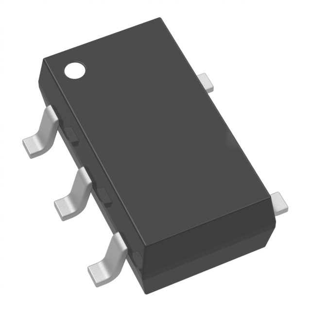
7. Pin-out (8-land USON 4 × 3)
TableCopy
| Pin # | Name | Function |
|---|---|---|
| 1 | CS# | Chip-select (active low) |
| 2 | SO/SIO1 | Data output (1-I/O) or SIO1 (2-/4-I/O) |
| 3 | WP#/SIO2 | Write-protect or SIO2 (4-I/O) |
| 4 | GND | Ground |
| 5 | SI/SIO0 | Data input (1-I/O) or SIO0 (2-/4-I/O) |
| 6 | SCLK | Serial clock |
| 7 | HOLD#/SIO3 | Hold (1-I/O) or SIO3 (4-I/O) |
| 8 | VCC | 2.3 V – 3.6 V supply Note: WP# & HOLD# have internal pull-high; exposed pad underneath must be connected to GND or left floating. |
8. Erase & Programming Times
TableCopy
| Operation | Typ. | Max. |
|---|---|---|
| Page Program (256 B) | 0.8 ms | 4 ms |
| Sector Erase (4 KB) | 38 ms | 240 ms |
| Block Erase (32 KB) | 0.23 s | 1.5 s |
| Block Erase (64 KB) | 0.45 s | 3 s |
| Chip Erase | 12 s | 38 s Times shorten ≈10 % when 7 V – 8 V is applied to WP# for high-voltage accelerate mode. |
9. Environmental & Reliability
- Industrial temperature: –40 °C to +85 °C
- Storage temperature: –65 °C to +150 °C
- Latch-up immunity: ±100 mA on any pin
- Moisture sensitivity: MSL-3 (USON)
- ESD HBM: 2 kV min
- RotHS, REACH, halogen-free, conflict-mineral free
10. Ordering Information
TableCopy
| Part Number | Package | Temp. | Packing |
|---|---|---|---|
| MX25V1635FZBI | 8-USON 4 × 3 mm | –40 °C to 85 °C | 3 k pcs reel (180 mm) |
| MX25V1635FZBI-TR | Same, tape & reel | – | 3 k |
| MX25V1635FZBI-S | Same, sample strip | – | 10 |
11. Reference Documents
- MX25V1635F Datasheet Rev. 1.4 (Macronix)
- JEDEC JESD216B SFDP specification supported
- Application notes: “Quad I/O Layout Guide”, “Suspend-Resume Usage”, “Secured OTP Programming”
Purchase
No need to register to order from JMBom Electronics, but signing in lets you track your order like a pro. Give it a try for a smoother shopping ride.
Means
Easy peasy! Pay your way with PayPal, Credit Card, or wire transfer in USD. We've got you covered.
RFQ(Request for Quotations)
Get the freshest prices and stock updates by asking for a quote! Our sales team will shoot you an email within a day. It's that simple.
IMPORTANT NOTICE
1. Look out for your order details in your inbox! (If it's missing, check the spam folder just in case.)
2. Our sales manager will double-check the order and keep you posted on any price or stock changes. No worries, we've got you covered.

Shipping Rate
We ship orders once a day around 5 p.m., except Sunday. Once shipped, the estimated delivery time depends on the courier company you choose, usually 5-7 working days.

Shipping Methods
We provide DHL, FedEx, UPS, EMS, SF Express, and Registered Air Mail international shipping.


Payment
You can pay the orders on the website directly or pay by wire transfer offline. We support: Paypal、VISA、Credit Card.


Macronix
Macronix
Macronix
Macronix
Macronix
Macronix
Macronix
Macronix
Macronix
Macronix
Macronix

Macronix