NXP PCA2002U/AB/1,026


- Part Number:
PCA2002U/AB/1,026
- Manufacturer:
- Category:
- RoHs:
 RoHS Compliant
 - Datasheet:
 PCA2002U/AB/1,026_Datesheet
 - Description:
IC WATCH CIRCUIT WAFER
- In stock 0

PCA2002U/AB/1,026 Device Information
Ordering Information
TableCopy
| Parameter | Description | Value |
|---|---|---|
| Type Number | Device identifier | PCA2002U/AB/1,026 |
| Topside Marking | Marking on the active side of the die | PC 2002-1 |
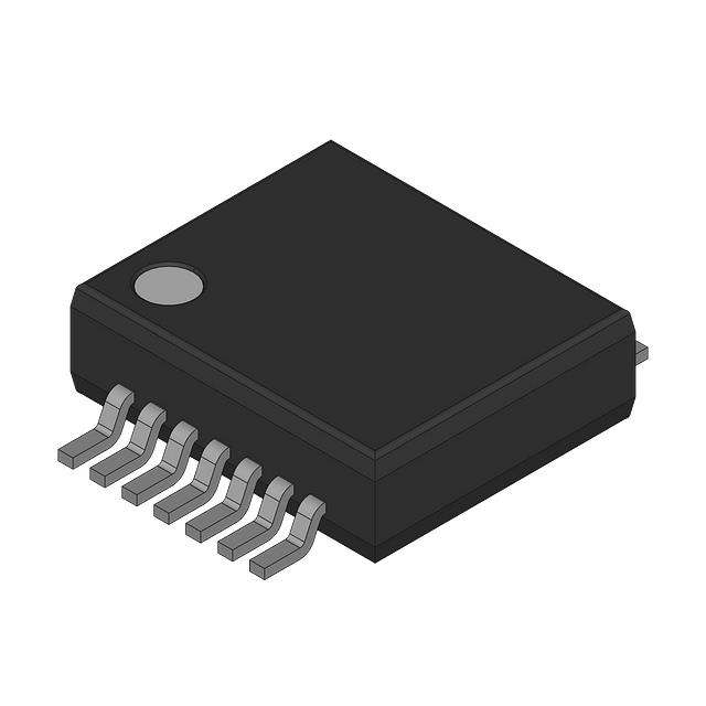
| Package | Physical package type | Wire bond die |
| Package Description | Detailed package description | 8 bonding pads; 1.16 × 0.86 × 0.22 mm |
| Version | Package version | PCA200xU |
Pinning Information
TableCopy
| Symbol | Pin Number | Description |
|---|---|---|
| Vss | 1 | Ground |
| i.c. | 2 | Internally connected (used for factory tests; should be left open-circuit in normal operation) |
| OSCIN | 3 | Oscillator input |
| OSCOUT | 4 | Oscillator output |
| VDD | 5 | Supply voltage |
| MOT1 | 6 | Motor 1 output |
| MOT2 | 7 | Motor 2 output |
| RESET | 8 | Reset input |
Functional Description
The PCA2002U/AB/1,026 is a CMOS integrated circuit designed for battery-operated wrist watches. It features a 32kHz quartz crystal oscillator and is optimized for minimum current consumption. The device includes programmable output periods and pulse widths, making it suitable for driving bipolar stepping motors.
Features and Benefits
- Amplitude-regulated 32kHz quartz crystal oscillator with excellent frequency stability and high immunity to leakage currents.
- Electrically programmable time calibration with 1ppm resolution stored in One Time Programmable (OTP) memory.
- Very low current consumption: typically 90nA.
- Output pulses for bipolar stepping motors.
- Five different programmable output periods (1s to 30s).
- Output pulse width programmable between 1ms and 8ms.
- Full or chopped motor pulse and pulse stretching.
- Stop function for accurate time setting and current saving during shelf life.
- Test mode for accelerated testing of the mechanical parts of the watch.
- Test bits for type recognition.
Limiting Values
TableCopy
| Parameter | Min | Max | Unit |
|---|---|---|---|
| Supply Voltage (VDD) | -1.8 | +7.0 | V |
| Input Voltage | -0.5 | +7.5 | V |
| Short Circuit Duration Time (tsc) | - | indefinite | S |
| Electrostatic Discharge Voltage (VESD) | - | ±2000 | V (HBM) |
| Electrostatic Discharge Voltage (VESD) | - | ±200 | V (MM) |
| Storage Temperature (Tstg) | -30 | +100 | °C |
| Ambient Temperature (Tamb) | -10 | +60 | °C |
Characteristics
TableCopy
| Parameter | Conditions | Min | Typ | Max | Unit |
|---|---|---|---|---|---|
| Supply Voltage (VDD) | Normal operating mode; Tamb = -10°C to +60°C | 1.1 | 1.55 | 3.6 | V |
| Supply Current (IDD) | Between motor pulses | - | 90 | 120 | nA |
| Saturation Voltage (Vsat) | Rmotor = 2 kΩ; Tamb = -10°C to +60°C | - | 150 | 200 | mV |
| Output Impedance (Zo(sc)) | Between motor pulses; Imotor < 1 mA | - | 200 | 300 | Ω |
| Oscillator Start Voltage (Vstart) | - | 1.1 | - | - | V |
| Frequency Stability (Δf/f) | ΔVDD = 100 mV | - | 0.05 | 0.2 | ppm |
| Integrated Load Capacitance (CL(itg)) | - | 5.2 | 6.3 | pF | |
| Parasitic Resistance (Rpar) | - | - | 20 | MΩ |
OTP Programming Characteristics
TableCopy
| Parameter | Conditions | Min | Typ | Max | Unit |
|---|---|---|---|---|---|
| Supply Voltage (VDD) | During programming procedure | 1.5 | - | 3.0 | V |
| Programming Supply Voltage (VP(prog)(start)) | - | 6.6 | - | 6.8 | V |
| Programming Supply Voltage (VP(prog)(stop)) | - | 6.2 | - | 6.4 | V |
| Supply Voltage Modulation (VP(mod)) | - | 320 | 350 | 380 | mV |
| Prestore Voltage (Vprestore) | - | 6.2 | - | 6.4 | V |
| Store Voltage (Vstore) | - | 9.9 | 10.0 | 10.1 | V |
| Store Current (Istore) | - | - | 10 | mA | |
| Start Pulse Width (tp(start)) | - | 8 | 10 | 12 | ms |
| Stop Pulse Width (tp(stop)) | - | 0.05 | - | 0.5 | ms |
| Modulation Pulse Width (tmod) | - | 25 | 30 | 40 | μs |
| Prestore Pulse Width (tw(prestore)) | - | 0.05 | - | 0.5 | ms |
| Store Pulse Width (tw(store)) | - | 95 | 100 | 110 | ms |
| Time 0 (t0) | Waiting time after start pulse | 20 | - | 30 | ms |
| Time 1 (t1) | Pulse distance for incrementing state counter | 0.6 | 0.7 | 0.8 | ms |
| Time 2 (t2) | Pulse distance for clocking data register with data = logic 0 | 1.6 | 1.7 | 1.8 | ms |
| Time 3 (t3) | Pulse distance for clocking data register with data = logic 1 | 2.6 | 2.7 | 2.8 | ms |
| Time 4 (t4) | Waiting time for writing to OTP cells | 0.1 | 0.2 | 0.3 | ms |
| Slew Rate (SR) | For modulation of supply voltage | 0.5 | - | 5.0 | V/μs |
| Modulation Resistance (Rmod) | - | 18 | 30 | 45 | kΩ |
Bare Die Outline
- Package Type: Wire bond die
- Dimensions: 1.16 × 0.86 × 0.22 mm
- Bonding Pads: 8 pads
Packing Information
- Orderable Part Number: PCA2002U/AB/1,026
- Package: Wire bond die
- Packing Method: Bare die; chip in tray
- Minimum Order Quantity: 36,000
- Temperature Range: Tamb = -10°C to +60°C
Purchase
No need to register to order from JMBom Electronics, but signing in lets you track your order like a pro. Give it a try for a smoother shopping ride.
Means
Easy peasy! Pay your way with PayPal, Credit Card, or wire transfer in USD. We've got you covered.
RFQ(Request for Quotations)
Get the freshest prices and stock updates by asking for a quote! Our sales team will shoot you an email within a day. It's that simple.
IMPORTANT NOTICE
1. Look out for your order details in your inbox! (If it's missing, check the spam folder just in case.)
2. Our sales manager will double-check the order and keep you posted on any price or stock changes. No worries, we've got you covered.

Shipping Rate
We ship orders once a day around 5 p.m., except Sunday. Once shipped, the estimated delivery time depends on the courier company you choose, usually 5-7 working days.

Shipping Methods
We provide DHL, FedEx, UPS, EMS, SF Express, and Registered Air Mail international shipping.


Payment
You can pay the orders on the website directly or pay by wire transfer offline. We support: Paypal、VISA、Credit Card.