


REF19x Series Precision Low-Dropout Voltage References
Catalog
OverviewKey FeaturesTypical ApplicationsTest PinsSpecificationsREF193 Electrical Characteristics (Quick Notes)APPLICATION NOTESConclusionOverview
The REF19x series precision band-gap voltage references use a patented circuit for correcting temperature drift curvature and employ laser-trimmed, highly stable thin-film resistors. This design ensures excellent initial accuracy and a very low temperature coefficient.
These devices are micropower, low dropout voltage (LDV) references, capable of delivering a stable output with supply voltages only 100 mV above the output level, while drawing less than 45 μA of supply current. When placed in sleep mode by applying a low TTL or CMOS signal to the SLEEP pin, the output is disabled and supply current drops to under 15 μA.

REF19x Series Precision Low-Dropout Voltage
The REF19x series is rated for operation across the extended industrial temperature range (−40°C to +85°C), with typical performance specifications extending to −40°C to +125°C, making them suitable for automotive and other demanding applications.
All electrical grades are offered in an 8-lead SOIC package, while PDIP and TSSOP packages are limited to the lowest electrical grade.
Key Features
- Temperature coefficient: up to 5 ppm/°C
- High output drive: 30 mA
- Low operating current: max 45 μA
- Initial accuracy: within ±2 mV¹
- Sleep mode: as low as 15 μA
- Low dropout operation
- Load regulation: 4 ppm/mA
- Line regulation: 4 ppm/V
- Built-in short-circuit protection
Typical Applications
- Portable measuring devices
- ADCs and DACs
- Intelligent sensors
- Solar-powered systems
- Loop-powered instruments
Test Pins
Test Pin 1 and Test Pin 5 are reserved for internal Zener zap adjustment.
The Zener zapping process is used to fine-tune the output voltage for maximum accuracy. Since each device may need a different level of correction, the resistance measured at these test pins can vary significantly from unit to unit. For this reason, users should leave Pin 1 and Pin 5 unconnected.
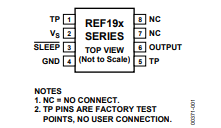
Figure 1. 8-Lead SOIC_N and TSSOP Pin Configuration
(S Suffix and RU Suffix)
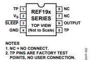
Figure 2. 8-Lead PDIP Pin Configuration
(P Suffix)
Specifications
Electrical Characteristics — REF191 @ TA = 25°C
Conditions: VS = 3.3 V, TA = 25°C, unless otherwise specified.
| Parameter | Symbol | Condition | Min | Typ | Max | Unit |
|---|---|---|---|---|---|---|
| Initial Accuracy¹ | VO | E Grade, IOUT = 0 mA | 2.046 | 2.048 | 2.050 | V |
| F Grade | 2.048 | 2.053 | V | |||
| G Grade | 2.048 | 2.058 | V | |||
| Line Regulation² | ΔVO/ΔVIN | E Grade, 3.0 V ≤ VS ≤ 15 V, IOUT = 0 mA | 2 | 4 | — | ppm/V |
| F & G Grades | 4 | 8 | — | ppm/V | ||
| Load Regulation² | ΔVO/ΔVLOAD | E Grade, VS = 5.0 V, 0–30 mA | 4 | 10 | — | ppm/mA |
| F & G Grades | 6 | 15 | — | ppm/mA | ||
| Dropout Voltage | VS − VO | VS = 3.0 V, ILOAD = 2 mA | — | 0.95 | — | V |
| VS = 3.3 V, ILOAD = 10 mA | — | 1.25 | — | V | ||
| VS = 3.6 V, ILOAD = 30 mA | — | 1.55 | — | V | ||
| Long-Term Stability³ | ΔVO | 1000 hours @ 125°C | — | 1.2 | — | mV |
| Noise Voltage | eN | 0.1 Hz to 10 Hz | — | 20 | — | μV p-p |
Notes:
- Initial accuracy does not account for shifts caused by solder heat (see Applications Information).
- Line and load regulation include the effects of self-heating.
- Long-term stability is noncumulative; drift in later 1000-hour intervals is much lower than during the first.
Electrical Characteristics — REF191 @ −40°C to +85°C
Conditions: VS = 3.3 V, −40°C ≤ TA ≤ +85°C, unless otherwise specified.
| Parameter | Symbol | Condition | Min | Typ | Max | Unit |
|---|---|---|---|---|---|---|
| Temperature Coefficient¹,² | TCVO/°C | E Grade, IOUT = 0 mA | 2 | — | 5 | ppm/°C |
| F Grade | 5 | — | 10 | ppm/°C | ||
| G Grade³ | 10 | — | 25 | ppm/°C | ||
| Line Regulation⁴ | ΔVO/ΔVIN | E Grade, 3.0 V ≤ VS ≤ 15 V, IOUT = 0 mA | 5 | — | 10 | ppm/V |
| F & G Grades | 10 | — | 20 | ppm/V | ||
| Load Regulation⁴ | ΔVO/ΔVLOAD | E Grade, VS = 5.0 V, 0–25 mA | 5 | — | 15 | ppm/mA |
| F & G Grades | 10 | — | 20 | ppm/mA | ||
| Dropout Voltage | VS − VO | VS = 3.0 V, ILOAD = 2 mA | — | 0.95 | — | V |
| VS = 3.3 V, ILOAD = 10 mA | — | 1.25 | — | V | ||
| VS = 3.6 V, ILOAD = 25 mA | — | 1.55 | — | V | ||
| Sleep Pin | VH | Logic High Input Voltage | 2.4 | — | — | V |
| IH | Logic High Input Current | — | −8 | — | μA | |
| VL | Logic Low Input Voltage | — | — | 0.8 | V | |
| IL | Logic Low Input Current | — | −8 | — | μA | |
| Supply Current | — | No load | — | 45 | — | μA |
| Sleep Mode Current | — | No load | — | 15 | — | μA |
Notes:
- A 1 μF capacitor is required between the output pin and GND for proper operation.
- TCVO is defined as the change in output voltage relative to temperature range, expressed in ppm/°C: TCVO=(VMAX−VMIN)/(VO×(TMAX−TMIN))TCVO = (VMAX − VMIN) / (VO × (TMAX − TMIN))TCVO=(VMAX−VMIN)/(VO×(TMAX−TMIN))
- G Grade values are guaranteed by characterization.
- Line and load regulation include the effects of self-heating.
Electrical Characteristics — REF191 @ −40°C to +125°C
Conditions: VS = 3.3 V, −40°C ≤ TA ≤ +125°C, unless otherwise specified.
| Parameter | Symbol | Condition | Min | Typ | Max | Unit |
|---|---|---|---|---|---|---|
| Temperature Coefficient¹,² | TCVO/°C | E Grade, IOUT = 0 mA | — | 2 | — | ppm/°C |
| F Grade | — | 5 | — | ppm/°C | ||
| G Grade³ | — | 10 | — | ppm/°C | ||
| Line Regulation⁴ | ΔVO/ΔVIN | E Grade, 3.0 V ≤ VS ≤ 15 V, IOUT = 0 mA | — | 10 | — | ppm/V |
| F & G Grades | — | 20 | — | ppm/V | ||
| Load Regulation⁴ | ΔVO/ΔVLOAD | E Grade, VS = 5.0 V, 0–20 mA | — | 10 | — | ppm/mA |
| F & G Grades | — | 20 | — | ppm/mA | ||
| Dropout Voltage | VS − VO | VS = 3.3 V, ILOAD = 10 mA | — | 1.25 | — | V |
| VS = 3.6 V, ILOAD = 20 mA | — | 1.55 | — | V |
Notes:
- A 1 μF capacitor between output and GND is required for correct operation.
- TCVO is the ratio of output voltage change to the specified temperature range, expressed in ppm/°C: TCVO=(VMAX−VMIN)/(VO×(TMAX−TMIN))TCVO = (VMAX − VMIN) / (VO × (TMAX − TMIN))TCVO=(VMAX−VMIN)/(VO×(TMAX−TMIN))
- G Grade values are guaranteed by characterization.
- Line and load regulation include self-heating effects.
Electrical Characteristics — REF192 @ TA = 25°C
Conditions: VS = 3.3 V, TA = 25°C, unless otherwise specified.
| Parameter | Symbol | Condition | Min | Typ | Max | Unit |
|---|---|---|---|---|---|---|
| Initial Accuracy¹ | VO | E Grade, IOUT = 0 mA | 2.498 | 2.500 | 2.502 | V |
| F Grade | 2.495 | — | 2.505 | V | ||
| G Grade | 2.490 | — | 2.510 | V | ||
| Line Regulation² | ΔVO/ΔVIN | E Grade, 3.0 V ≤ VS ≤ 15 V, IOUT = 0 mA | 2 | 4 | — | ppm/V |
| F & G Grades | 4 | 8 | — | ppm/V | ||
| Load Regulation² | ΔVO/ΔVLOAD | E Grade, VS = 5.0 V, 0–30 mA | 4 | 10 | — | ppm/mA |
| F & G Grades | 6 | 15 | — | ppm/mA | ||
| Dropout Voltage | VS − VO | VS = 3.5 V, ILOAD = 10 mA | — | 1.00 | — | V |
| VS = 3.9 V, ILOAD = 30 mA | — | 1.40 | — | V | ||
| Long-Term Stability³ | ΔVO | 1000 hours @ 125°C | — | 1.2 | — | mV |
| Noise Voltage | eN | 0.1 Hz to 10 Hz | — | 25 | — | μV p-p |
Notes:
- Initial accuracy does not include shifts caused by soldering heat (see Applications Information).
- Line and load regulation include the effects of self-heating.
- Long-term stability is noncumulative; drift in later 1000-hour intervals is significantly lower than during the first 1000-hour period.
Electrical Characteristics — REF192 @ −40°C to +85°C
Conditions: VS = 3.3 V, −40°C ≤ TA ≤ +85°C, unless otherwise noted.
| Parameter | Symbol | Condition | Min | Typ | Max | Unit |
|---|---|---|---|---|---|---|
| Temperature Coefficient¹,² | TCVO/°C | E Grade, IOUT = 0 mA | 2 | — | 5 | ppm/°C |
| F Grade | 5 | — | 10 | ppm/°C | ||
| G Grade³ | 10 | — | 25 | ppm/°C | ||
| Line Regulation⁴ | ΔVO/ΔVIN | E Grade, 3.0 V ≤ VS ≤ 15 V, IOUT = 0 mA | 5 | — | 10 | ppm/V |
| F & G Grades | 10 | — | 20 | ppm/V | ||
| Load Regulation⁴ | ΔVO/ΔVLOAD | E Grade, VS = 5.0 V, 0–25 mA | 5 | — | 15 | ppm/mA |
| F & G Grades | 10 | — | 20 | ppm/mA | ||
| Dropout Voltage | VS − VO | VS = 3.5 V, ILOAD = 10 mA | — | 1.00 | — | V |
| VS = 4.0 V, ILOAD = 25 mA | — | 1.50 | — | V | ||
| Sleep Pin | VH | Logic High Input Voltage | 2.4 | — | — | V |
| IH | Logic High Input Current | — | −8 | — | μA | |
| VL | Logic Low Input Voltage | — | — | 0.8 | V | |
| IL | Logic Low Input Current | — | −8 | — | μA | |
| Supply Current | — | No load | — | 45 | — | μA |
| Sleep Mode Current | — | No load | — | 15 | — | μA |
Electrical Characteristics — REF192 @ −40°C to +125°C
Conditions: VS = 3.3 V, −40°C ≤ TA ≤ +125°C, unless otherwise noted.
| Parameter | Symbol | Condition | Min | Typ | Max | Unit |
|---|---|---|---|---|---|---|
| Temperature Coefficient¹,² | TCVO/°C | E Grade, IOUT = 0 mA | — | 2 | — | ppm/°C |
| F Grade | — | 5 | — | ppm/°C | ||
| G Grade³ | — | 10 | — | ppm/°C | ||
| Line Regulation⁴ | ΔVO/ΔVIN | E Grade, 3.0 V ≤ VS ≤ 15 V, IOUT = 0 mA | — | 10 | — | ppm/V |
| F & G Grades | — | 20 | — | ppm/V | ||
| Load Regulation⁴ | ΔVO/ΔVLOAD | E Grade, VS = 5.0 V, 0–20 mA | — | 10 | — | ppm/mA |
| F & G Grades | — | 20 | — | ppm/mA | ||
| Dropout Voltage | VS − VO | VS = 3.5 V, ILOAD = 10 mA | — | 1.00 | — | V |
| VS = 4.0 V, ILOAD = 20 mA | — | 1.50 | — | V |
Notes (for both tables):
- A 1 μF capacitor between the output pin and GND is required for proper operation.
- TCVO is defined as the ratio of output change with temperature variation over the specified range, in ppm/°C: TCVO=(VMAX−VMIN)/(VO×(TMAX−TMIN))TCVO = (VMAX − VMIN) / (VO × (TMAX − TMIN))TCVO=(VMAX−VMIN)/(VO×(TMAX−TMIN))
- G Grade values are guaranteed by characterization.
- Line and load regulation include the effects of self-heating.
REF193 Electrical Characteristics (Quick Notes)
At 25°C, VS = 3.3 V
- Initial Accuracy: Output around 3.0 V (2.990 to 3.010 V).
- Line Regulation: Very stable, 4 to 8 ppm/V change with input variations.
- Load Regulation: About 6 to 15 ppm/mA with load changes up to 30 mA.
- Dropout Voltage: 0.80 V @ 10 mA load (with 3.8 V supply). 1.00 V @ 30 mA load (with 4.0 V supply).
- Long-Term Stability: Only about 1.2 mV drift after 1000 hours at 125°C (first period is the biggest shift, later ones are much smaller).
- Noise: 30 µV peak-to-peak in the 0.1 Hz to 10 Hz range.
Across −40°C to +85°C, VS = 3.3 V
- Temperature Coefficient (TC): Around 10 to 25 ppm/°C (how much output drifts per degree).
- Line Regulation: 10 to 20 ppm/V.
- Load Regulation: 10 to 20 ppm/mA (up to 25 mA).
- Dropout Voltage: 0.80 V @ 10 mA load (with 3.8 V supply). 1.10 V @ 30 mA load (with 4.1 V supply).
- Sleep Pin: Logic High: ≥2.4 V (input current ~ −8 µA). Logic Low: ≤0.8 V (input current ~ −8 µA).
- Supply Current: ~45 µA normal, 15 µA in sleep mode.
Note: Always place a 1 µF capacitor between output and ground for stable operation.
In short, REF193 is a precise 3.0 V reference with low drift, low power use, and small dropout voltage, making it great for battery-powered and precision circuits.
Absolute Maximum Ratings (REF19x)
- Supply Voltage: From −0.3 V up to +18 V.
- Output to Ground: −0.3 V to (VS + 0.3 V).
- Output Short-Circuit: Can handle indefinite short to ground (protected).
- Storage Temp (PDIP, SOIC): −65°C to +150°C.
- Operating Temp (REF19x): −40°C to +125°C.
- Junction Temp (PDIP, SOIC): −65°C to +150°C.
- Soldering (Lead, 60 sec): Up to 300°C.
Important Note:
- These are absolute stress limits, not recommended operating values.
- Exceeding them may permanently damage the device.
- Running at or near these limits for a long time can also reduce reliability, even if the chip still works.
Thermal Resistance
The value of θJA (junction-to-ambient thermal resistance) is given under worst-case conditions:
- For PDIP packages, it is measured with the device placed in a socket.
- For SOIC and TSSOP packages, it is measured with the device soldered directly to the circuit board.
Table 24. Thermal Resistance Values
| Package Type | θJA (°C/W) | θJC (°C/W) |
|---|---|---|
| 8-Lead PDIP (N) | 103 | 43 |
| 8-Lead SOIC (R) | 158 | 43 |
| 8-Lead TSSOP (RU) | 240 | 43 |
In short:
- Lower θJA = better heat dissipation.
- PDIP handles heat best, while TSSOP has the highest thermal resistance, meaning it runs hotter under the same power conditions.
APPLICATION NOTES
Output Short-Circuit Protection
The REF19x series is fully safeguarded against damage caused by accidental short circuits to GND or VS. If a short-circuit occurs, the device automatically shuts down and restricts its supply current to 40 mA.
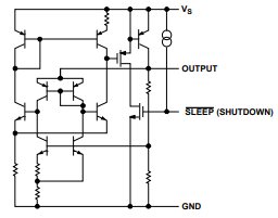
Simplified Schematic
DEVICE POWER DISSIPATION CONSIDERATIONS
The REF19x series can supply load currents up to 30 mA with input voltages ranging from 3.3 V to 15 V. When operating at higher input voltages, care should be taken to avoid exceeding the device’s maximum internal power dissipation. Surpassing the specified limits for power dissipation or junction temperature may lead to premature device failure. The maximum junction temperature or power dissipation can be calculated using the following formula:TJ=TA+PD×θJAT_J = T_A + P_D \times \theta_{JA}TJ=TA+PD×θJA
where TJT_JTJ is the junction temperature, TAT_ATA is the ambient temperature, PDP_DPD is the device power dissipation, and θJA\theta_{JA}θJA is the thermal resistance of the device package.
OUTPUT VOLTAGE BYPASSING
For stable operation, low-dropout voltage regulators and references typically require a bypass capacitor between the VOUT and GND pins. The REF19x series can maintain stable operation with capacitive loads above 100 μF, though a 1 μF capacitor is sufficient to ensure rated performance. Adding a 0.1 μF ceramic capacitor in parallel with the bypass capacitor enhances load transient response.
For optimal line voltage transient performance, it is recommended to bypass the device’s input with a 10 μF electrolytic capacitor in parallel with a 0.1 μF ceramic capacitor.
SLEEP MODE OPERATION
All REF19x devices feature a sleep function compatible with TTL/CMOS logic levels. Internally, a pull-up current source to VS is connected to the SLEEP pin, allowing it to be controlled by an open-collector or open-drain driver. Driving the SLEEP pin low (0 V) turns off the output stage. In sleep mode, the reference output goes into a high-impedance state, with its voltage determined by external circuitry. If the sleep function is not used, the SLEEP pin should be tied to VS (Pin 2).
BASIC VOLTAGE REFERENCE CONNECTIONS
Picture shows the standard configuration for the REF19x series. The input features a 10 μF/0.1 μF bypass network, while the output uses a 1 μF/0.1 μF bypass network. Pins 1, 5, 7, and 8 should remain unconnected. If the sleep feature is not needed, Pin 3 should be connected to VS.
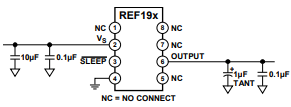
Basic Voltage Reference Connections
MEMBRANE SWITCH–CONTROLLED POWER SUPPLY
The REF19x series can function as a low-dropout power supply in handheld instruments with output currents in the tens of milliamps. In the circuit shown in Figure 22, a membrane on/off switch controls the reference operation.
At initial power-on, the SLEEP pin is held low through a 10 kΩ resistor, placing the REF19x output in a high-impedance (three-state) condition. Pressing the membrane on switch momentarily pulls the SLEEP pin to VS, enabling the REF19x output. At this point, current through the 10 kΩ resistor decreases, and the internal current source connected to the SLEEP pin takes over, keeping Pin 3 at VS. Pressing the membrane off switch momentarily connects the SLEEP pin to GND, once again disabling the REF19x output.
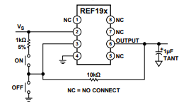
Membrane Switch Controlled Power Supply
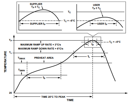
Classification Profile (Not to Scale)
SOLDER HEAT EFFECT
The mechanical stress and heat from soldering a device to a PCB can cause the reference output voltage to shift. For example, the output voltage of the REF195 changes after exposure to the high temperatures of a lead-free soldering profile, such as the one shown in Picture.
The semiconductor die and package materials expand and contract at different rates, creating stress on the die during soldering and resulting in an output voltage shift. This effect is similar to, but more pronounced than, thermal hysteresis.Picture illustrates a typical output voltage shift caused by soldering temperatures, excluding any mechanical stress effects.
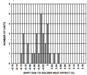
Output Shift due to Solder Heat Effect
Conclusion
The REF19x series offers highly precise, low-power, and low-dropout voltage references suitable for a wide range of demanding applications, including portable instruments, ADCs/DACs, and automotive systems. With excellent initial accuracy, low temperature drift, robust short-circuit protection, and a controllable sleep mode, these devices ensure reliable and stable voltage output across extended temperature ranges. Proper thermal management, capacitor bypassing, and attention to soldering effects are important to maintain performance and long-term stability. Overall, the REF19x series provides a versatile and dependable solution for precision voltage reference needs.

Amanda Miller
Amanda Miller is a senior electronics engineer with 6 years of experience. She focuses on studying resistors, transistors, and package design in detail. Her deep knowledge helps her bring innovation and high standards to the electronics industry.
Subscribe to JMBom Electronics !


