
Analog Devices Inc.(ADI) ADL5566ACPZ-R7


- Part Number:
ADL5566ACPZ-R7
- Manufacturer:
- Category:
- RoHs:
 RoHS Compliant
 - Datasheet:
 ADL5566ACPZ-R7_Datesheet
 - Description:
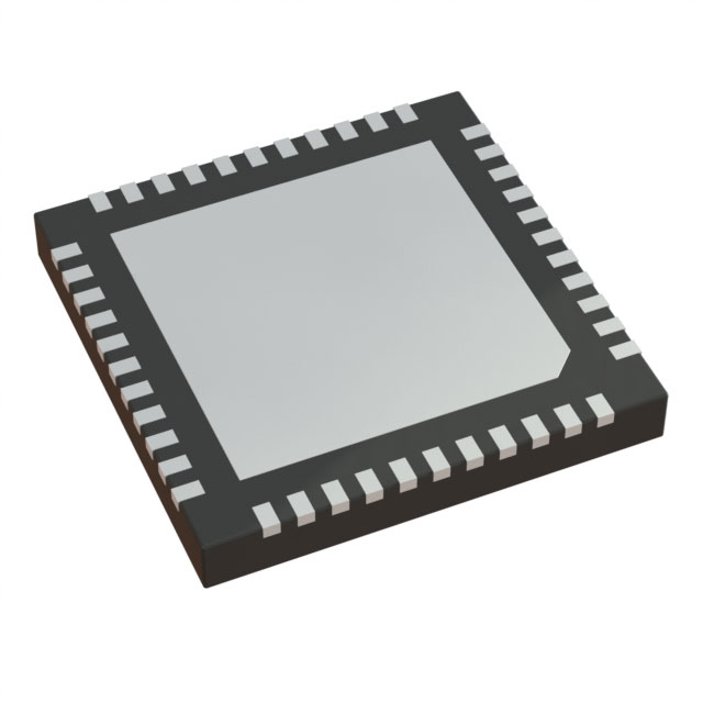
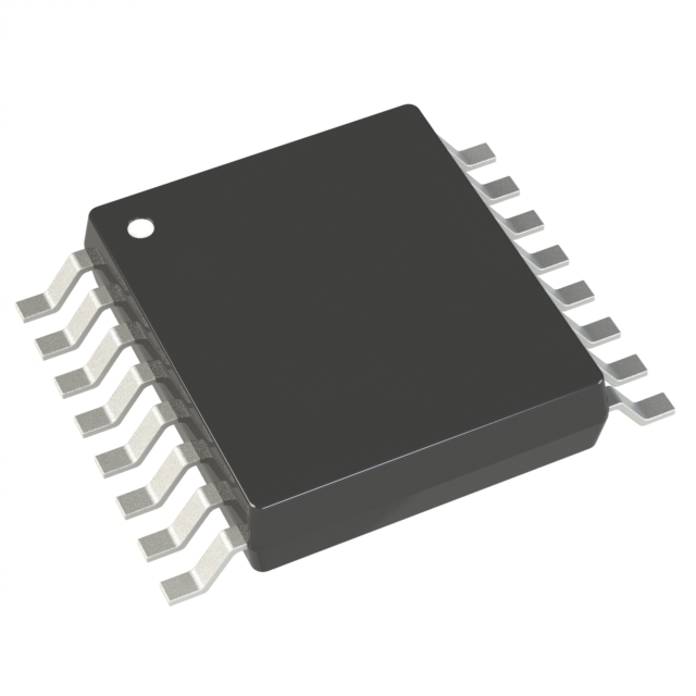
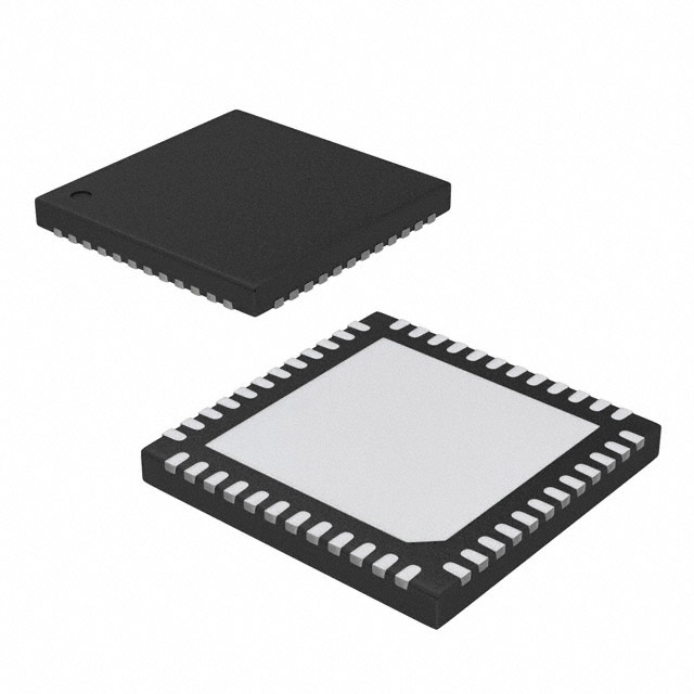
IC OPAMP RF/IF DIFF 2CIR 24LFCSP
- In stock 877

ADL5566ACPZ‑R7 – Complete Datasheet Summary
1. Basic Device Information
- Part Number: ADL5566ACPZ‑R7
- Manufacturer: Analog Devices Inc.
- Device Type: Dual‑Channel, Ultrahigh Dynamic Range Differential Amplifier / ADC Driver
- Frequency Range: DC to 4.5 GHz (−3 dB bandwidth)
- Fixed Gain: 16 dB (differential); 14 dB (single‑ended)
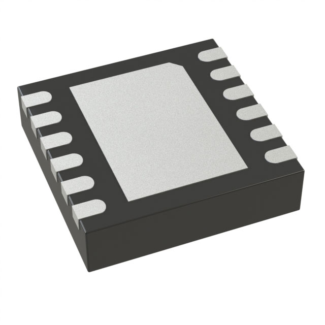
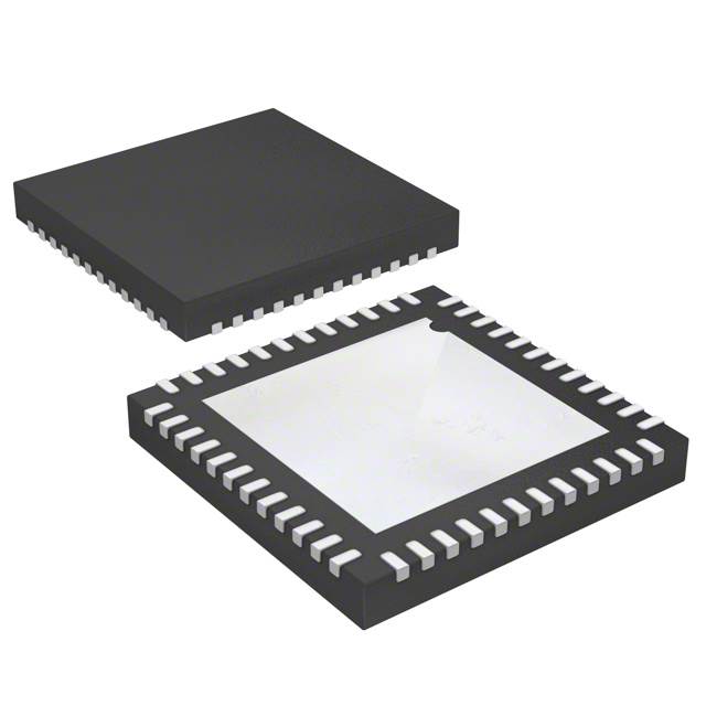
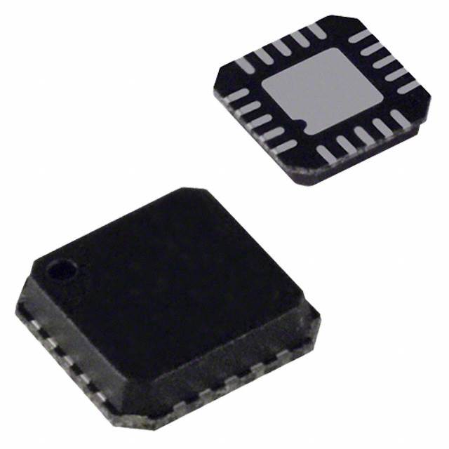
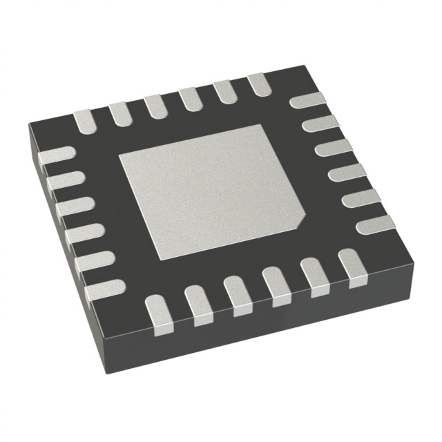
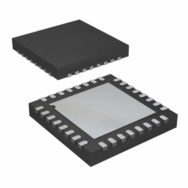
- Package: 24‑Lead LFCSP (4 mm × 4 mm, CP‑24‑14)
- Packaging: 7‑inch Tape and Reel
- RoHS: Compliant (Z suffix)
- Revision: Rev. C
- Operating Temperature: −40°C to +85°C
- Process: High‑Speed SiGe
2. Key Features
- −3 dB bandwidth: 4.5 GHz at AV = 16 dB
- Low input noise: 1.3 nV/√Hz RTI
- Ultra‑low distortion:
- Slew rate: 16 V/ns
- Settling time: 890 ps (2 V step to 1%)
- Overdrive recovery: 2.5 ns
- Single supply: 2.8 V to 5.2 V
- Power‑down mode: < 3.5 mA per channel
- Low power: 462 mW at 3.3 V
- Differential or single‑ended input → differential output
- DC‑coupled or AC‑coupled I/O
- Adjustable gain (0 dB to 16 dB differential) using external resistors
- Excellent channel matching:
- Low output common‑mode capability down to 1.2 V
3. Electrical Specifications (TA = 25°C, RL = 200 Ω differential, CL = 1 pF)
Supply & Operating Conditions
| Parameter | Min | Typ | Max | Unit |
|---|---|---|---|---|
| Supply Voltage (VCC) | 2.8 | 3.3 / 5.0 | 5.2 | V |
| Quiescent Current (per amp) | — | 70 | — | mA |
| Total IQ (both amps) | — | 140 | 160 | mA |
| Power‑Down Current | — | < 3.5 | — | mA |
Dynamic Performance
| Parameter | Typ | Max | Unit |
|---|---|---|---|
| −3 dB Bandwidth | 4500 | — | MHz |
| 0.1 dB Flatness Bandwidth | 500 | — | MHz |
| Gain Accuracy | — | ±1 | dB |
| Channel‑to‑Channel Gain Error | — | ≤0.02 | dB |
| Channel‑to‑Channel Phase Error | — | ≤0.5 | Deg |
| Reverse Isolation (S12) | 75 | — | dB |
| Channel Isolation | 82.5 | — | dB |
| CMRR | 44 | — | dB |
Input / Output Characteristics
| Parameter | Value | Unit |
|---|---|---|
| Differential Input Resistance | 160 | Ω |
| Single‑Ended Input Resistance | 150 | Ω |
| Input Capacitance | 1.1 | pF |
| Differential Output Resistance | 11 | Ω |
| Max Output Swing (1 dB compression) | 3.4 (3.3 V) / 5.0 (5 V) | V p‑p |
| Output Common‑Mode Range (3.3 V) | 1.25 to 1.8 | V |
| Output Common‑Mode Range (5 V) | 1.25 to 3.0 | V |
Noise & Distortion
| Parameter | Typ | Unit |
|---|---|---|
| Input Noise Density | 1.3 | nV/√Hz |
| Noise Figure (AV = 16 dB) | 6.5 | dB |
| OIP3 at 200 MHz | +46 | dBm |
| OP1dB at 100 MHz | 14.2 (3.3 V) / 17.8 (5 V) | dBm |
4. Absolute Maximum Ratings
- Supply Voltage (VCC): 5.25 V
- Input Voltage (VIPx, VINx): VCC + 0.5 V
- Max Output Current: ±30 mA
- Power Dissipation: 900 mW
- Junction Temperature: 135°C
- Storage Temperature: −65°C to +150°C
- ESD Sensitivity: ESD‑sensitive device
5. Thermal Resistance
| Parameter | Value | Unit |
|---|---|---|
| θJA (Junction‑to‑Ambient) | 34.0 | °C/W |
| θJC (Junction‑to‑Case) | 1.8 | °C/W |
6. Pin Configuration (24‑Lead LFCSP)
| Pin(s) | Name | Function |
|---|---|---|
| 1, 2 | VIN1, VIP1 | Differential Inputs, Amp 1 |
| 5, 6 | VIP2, VIN2 | Differential Inputs, Amp 2 |
| 17, 18 | VOP1, VON1 | Differential Outputs, Amp 1 |
| 13, 14 | VOP2, VON2 | Differential Outputs, Amp 2 |
| 20, 11 | VCC1, VCC2 | Positive Supply |
| 22, 9 | ENBL1, ENBL2 | Enable Pins (Active High) |
| 21, 10 | VCOM1, VCOM2 | Output Common‑Mode Adjust |
| 3, 4, 7, 8, 12, 15, 16, 19, 23, 24 | NC | No Connect |
| EP | Exposed Pad | Internal GND; must solder to GND plane |
7. Functional Description
- Dual independent differential amplifiers
- Fixed gain of 16 dB (diff) / 14 dB (SE)
- Gain adjustable 0–16 dB using external series resistors
- VCOMx sets output common‑mode voltage (defaults to VCC/2 if open)
- ENBLx enables/disables each channel independently
- Internal resistors set fixed gain; external resistors reduce gain
- Optimized for high‑speed ADC driving, differential conversion, and IF/RF gain blocks
8. Application Information
Typical Applications
- High‑speed differential ADC drivers
- Single‑ended to differential conversion
- IF / RF gain blocks
- SAW filter and analog front‑end interfaces
- Zero‑IF / complex‑IF receivers
- Test & measurement equipment
Basic Application Requirements
- Decouple VCC1/VCC2 with 0.1 µF + 10 µF capacitors
- Decouple VCOM1/VCOM2 with 0.1 µF capacitors
- Drive ENBL high to enable; low to power down
- Use 200 Ω differential load for rated distortion performance
- Input/output can be AC‑ or DC‑coupled
Gain Adjustment
- Place series resistors at inputs to reduce gain from 16 dB down to 0 dB
- Equations and lookup tables provided for desired gain vs. series resistance
9. Layout Guidelines
- Exposed pad must be soldered to low‑impedance ground plane
- Use multiple vias to connect pad to internal ground layers
- Keep input/output traces short; minimize parasitic capacitance
- Use ground planes to reduce noise and crosstalk
- Follow RF/high‑speed layout practices for wideband performance
10. Package & Mechanical Data
- Package Type: 24‑Lead LFCSP (CP‑24‑14)
- Body Size: 4.0 mm × 4.0 mm
- Height: 0.75 mm
- Coplanarity: 0.08 mm max
- JEDEC Standard: MO‑220‑WGGD‑8
- Marking: ADL5566
11. Ordering Information
- ADL5566ACPZ‑R7: −40°C to +85°C, 24‑LFCSP, 7‑inch reel
- ADL5566‑EVALZ: Evaluation Board
Purchase
No need to register to order from JMBom Electronics, but signing in lets you track your order like a pro. Give it a try for a smoother shopping ride.
Means
Easy peasy! Pay your way with PayPal, Credit Card, or wire transfer in USD. We've got you covered.
RFQ(Request for Quotations)
Get the freshest prices and stock updates by asking for a quote! Our sales team will shoot you an email within a day. It's that simple.
IMPORTANT NOTICE
1. Look out for your order details in your inbox! (If it's missing, check the spam folder just in case.)
2. Our sales manager will double-check the order and keep you posted on any price or stock changes. No worries, we've got you covered.

Shipping Rate
We ship orders once a day around 5 p.m., except Sunday. Once shipped, the estimated delivery time depends on the courier company you choose, usually 5-7 working days.

Shipping Methods
We provide DHL, FedEx, UPS, EMS, SF Express, and Registered Air Mail international shipping.


Payment
You can pay the orders on the website directly or pay by wire transfer offline. We support: Paypal、VISA、Credit Card.


Analog Devices Inc.(ADI)
Analog Devices Inc.(ADI)
Analog Devices Inc.(ADI)
Analog Devices Inc.(ADI)
Analog Devices Inc.(ADI)
Analog Devices Inc.(ADI)
Analog Devices Inc.(ADI)
Analog Devices Inc.(ADI)
Analog Devices Inc.(ADI)
Analog Devices Inc.(ADI)
Analog Devices Inc.(ADI)
Analog Devices Inc.(ADI)